KA555D Fairchild Semiconductor, KA555D Datasheet - Page 4
KA555D
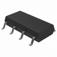
Manufacturer Part Number
KA555D
Description
IC TIMER CONTROLLER SGL 8-SOP
Manufacturer
Fairchild Semiconductor
Type
555 Type, Timer/Oscillator (Single)r
Datasheet
1.KA555IDTF.pdf
(14 pages)
Specifications of KA555D
Voltage - Supply
4.5 V ~ 16 V
Current - Supply
7.5mA
Operating Temperature
0°C ~ 70°C
Package / Case
8-SOIC (3.9mm Width)
Frequency
100kHz
Lead Free Status / RoHS Status
Lead free / RoHS Compliant
Count
-
Available stocks
Company
Part Number
Manufacturer
Quantity
Price

Part Number:
KA555D
Manufacturer:
FAIRCHILD/仙童
Quantity:
20 000
Company:
Part Number:
KA555DTF
Manufacturer:
JRC
Quantity:
41 283


KA555
KA555
KA555
KA555
Application Information
Application Information
Application Information
Application Information
Table1 below is the basic operating table of 555 timer:
When the low signal input is applied to the reset terminal, the timer output remains low regardless of the threshold voltage or
the trigger voltage. Only when the high signal is applied to the reset terminal, the timer's output changes according to
threshold voltage and trigger voltage.
When the threshold voltage exceeds 2/3 of the supply voltage while the timer output is high, the timer's internal discharge Tr.
turns on, lowering the threshold voltage to below 1/3 of the supply voltage. During this time, the timer output is maintained
low. Later, if a low signal is applied to the trigger voltage so that it becomes 1/3 of the supply voltage, the timer's internal
discharge Tr. turns off, increasing the threshold voltage and driving the timer output again at high
1. MonoStable Operation
1. MonoStable Operation
1. MonoStable Operation
1. MonoStable Operation
4 4 4 4
Vcc / 3 < V
Threshold Voltage
Threshold Voltage
Threshold Voltage
Threshold Voltage
Trigger
Figure 3. Waveforms of Monostable Operation
Figure 3. Waveforms of Monostable Operation
Figure 3. Waveforms of Monostable Operation
Figure 3. Waveforms of Monostable Operation
V
V
th
(V (V (V (V
Don't care
th
R
L
th th th th
> 2Vcc / 3
Figure 1. Monoatable Circuit
Figure 1. Monoatable Circuit
Figure 1. Monoatable Circuit
Figure 1. Monoatable Circuit
< Vcc / 3
)(Pin6)
)(Pin6)
)(Pin6)
)(Pin6)
th
< 2 Vcc / 3
3
2
OUT
TRIG
RESET
4
GND
1
Vcc / 3 < V
Trigger Voltage
Trigger Voltage
Trigger Voltage
Trigger Voltage
THRES
V
Vcc
DISCH
V
CONT
8
th
(V (V (V (V
Don't care
th
> 2Vcc / 3
tr tr tr tr
< Vcc / 3
)(Pin2)
)(Pin2)
)(Pin2)
)(Pin2)
th
7
6
5
Table 1. Basic Operating Table
Table 1. Basic Operating Table
Table 1. Basic Operating Table
Table 1. Basic Operating Table
< 2 Vcc / 3
C2
+Vcc
R
C1
A
Reset(Pin4)
Reset(Pin4)
Reset(Pin4)
Reset(Pin4)
High
High
High
Low
Figure 2. Resistance and Capacitance vs.
Figure 2. Resistance and Capacitance vs.
Figure 2. Resistance and Capacitance vs.
Figure 2. Resistance and Capacitance vs.
10 10 10 10
10 10 10 10
10 10 10 10
10 10 10 10
10 10 10 10
10 10 10 10
-1 -1 -1 -1
-2 -2 -2 -2
-3 -3 -3 -3
2 2 2 2
1 1 1 1
0 0 0 0
10 10 10 10
-5 -5 -5 -5
Time delay(t
Time delay(t
Time delay(t
Time delay(t
10 10 10 10
-4 -4 -4 -4
Output(Pin3)
Output(Pin3)
Output(Pin3)
Output(Pin3)
10 10 10 10
-3 -3 -3 -3
High
Low
Low
-
Time Delay(s)
Time Delay(s)
Time Delay(s)
Time Delay(s)
10 10 10 10
d d d d
-2 -2 -2 -2
) ) ) )
10 10 10 10
-1 -1 -1 -1
10 10 10 10
Discharging Tr.
Discharging Tr.
Discharging Tr.
Discharging Tr.
0 0 0 0
(Pin7)
(Pin7)
(Pin7)
(Pin7)
10 10 10 10
OFF
ON
ON
1 1 1 1
-
10 10 10 10
2 2 2 2
Related parts for KA555D
Image
Part Number
Description
Manufacturer
Datasheet
Request
R

Part Number:
Description:
IC TIMER CONTROLLER SGL 8-DIP
Manufacturer:
Fairchild Semiconductor
Datasheet:

Part Number:
Description:
Fairchild Semiconductor [IGBT MODULE]
Manufacturer:
Fairchild Semiconductor
Datasheet:

Part Number:
Description:
Discrete Semiconductor Modules
Manufacturer:
Fairchild Semiconductor
Part Number:
Description:
Discrete Semiconductor Modules
Manufacturer:
Fairchild Semiconductor
Part Number:
Description:
This N-Channel MOSFET is produced using Fairchild Semiconductor’s advanced Power Trench® process
Manufacturer:
Fairchild Semiconductor
Datasheet:
Part Number:
Description:
This N-Channel MOSFET is produced using Fairchild Semiconductor’s advanced Power Trench® process
Manufacturer:
Fairchild Semiconductor
Datasheet:
Part Number:
Description:
This N-Channel MOSFET is produced using Fairchild Semiconductor’s advanced PowerTrench® process
Manufacturer:
Fairchild Semiconductor
Datasheet:
Part Number:
Description:
This N-Channel MOSFET is produced using Fairchild Semiconductor’s advanced PowerTrench® process
Manufacturer:
Fairchild Semiconductor
Datasheet:
Part Number:
Description:
This N-Channel MOSFET is produced using Fairchild Semiconductor’s advanced Power Trench® process
Manufacturer:
Fairchild Semiconductor
Datasheet:
Part Number:
Description:
This N-Channel logic Level MOSFETs are produced using Fairchild Semiconductor‘s advanced Power Trench® process that has been special tailored to minimize the on-state resistance and yet maintain superior switching performance
Manufacturer:
Fairchild Semiconductor
Datasheet:
Part Number:
Description:
This N-Channel MOSFET is produced using Fairchild Semiconductor’s advanced Power Trench® process
Manufacturer:
Fairchild Semiconductor
Datasheet:
Part Number:
Description:
This N-Channel SyncFET™ is produced using Fairchild Semiconductor’s advanced PowerTrench® process
Manufacturer:
Fairchild Semiconductor
Datasheet:
Part Number:
Description:
This N-Channel SyncFET™ is produced using Fairchild Semiconductor’s advanced PowerTrench® process
Manufacturer:
Fairchild Semiconductor
Datasheet:
Part Number:
Description:
This N-Channel SyncFET™ is produced using Fairchild Semiconductor’s advanced PowerTrench® process
Manufacturer:
Fairchild Semiconductor
Datasheet:
Part Number:
Description:
This N-Channel logic Level MOSFETs are produced using Fairchild Semiconductor‘s advanced Power Trench® process that has been special tailored to minimize the on-state resistance and yet maintain superior switching performance
Manufacturer:
Fairchild Semiconductor
Datasheet: