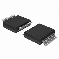
74LV4799DB,118 NXP Semiconductors, 74LV4799DB,118 Datasheet - Page 10

74LV4799DB,118
Manufacturer Part Number
74LV4799DB,118
Description
IC TIMER NICD/NIMH CHRGR 16SSOP
Manufacturer
NXP Semiconductors
Type
Timer Controlr
Series
74LVr
Datasheet
1.74LV4799SD118.pdf
(18 pages)
Specifications of 74LV4799DB,118
Package / Case
16-SSOP
Frequency
100kHz
Voltage - Supply
0.9 V ~ 6 V
Current - Supply
36µA
Operating Temperature
0°C ~ 70°C
Supply Voltage (max)
6 V
Supply Voltage (min)
0.9 V
Maximum Operating Temperature
+ 70 C
Minimum Operating Temperature
0 C
Mounting Style
SMD/SMT
Lead Free Status / RoHS Status
Lead free / RoHS Compliant
Count
-
Lead Free Status / RoHS Status
Lead free / RoHS Compliant, Lead free / RoHS Compliant
Other names
74LV4799DB-T
74LV4799DB-T
935175040118
74LV4799DB-T
935175040118
Philips Semiconductors
Charge discharge times
LED frequency
The frequency of the LED output (pin1) is determined by the oscillator frequency.
Three modes of operation, each with its own frequency, are possible.
MOLLI pulse duration
The MOLLI output gives an output signal of four periods with a 50%
duty cycle. The duration of one period is determined by: 16/f
Timing accuracy.
The timing accuracy depends on the accuracy of the on–chip
oscillator and on the external R and C components. The inaccuracy
of the on–chip oscillator is specified as maximum +/–7%. In most
cases the actual inaccuracy will be significantly lower. This depends
on the supply voltage as well as the value of the external
components.
Influence of Resistor value.
Low resistor values cause some spread because the RC
combination is biased by a 3–State push–pull output. The spread of
SPREAD-CAUSING FACTORS
1998 Apr 20
Charge time
Discharge time
Self-discharge time
Timer for NiCd and NiMH chargers
SYMBOL
SYMBOL
R
R
R
R
R
R
R
R
V
V
t
t
ON
ON
ON
ON
ON
ON
ON
ON
off
P
P
ff
PARAMETER
Trickle charge
Charge
Mode
Alarm
Offset voltage
Offset voltage
Propagation delay
Pro agation delay
P-channel resistance R
P-channel resistance R
N-channel resistance R
N-channel resistance R
P-channel resistance R
P-channel resistance R
N-channel resistance R
N-channel resistance R
PARAMETER
PARAMETER
C
C
C
C
S
S
S
S
, R
, R
output
out ut
output
out ut
R
R
4 hours to 16 hours
15 minutes to to 4.7 hours
50 days to 100 days
D
D
D
D
outputs
out uts
outputs
out uts
s
TIME RANGE
H or open
SEL
10
H
L
the R
spread. When high–value resistors are used, any possible output
leakage of the not–selected 3–State outputs will cause a frequency
deviation. For these reasons, the resistor values must be within the
specified ranges.
Influence of supply voltage
The trip levels of the oscillator are fixed at 20% and 80% of V
higher supply voltages the spread of the trip levels decreases in
greater proportion because the offset voltage remains constant, and
the propagation delay decreases. Furthermore, the R
the push–pull driving stage decrease at higher voltages.
on
V
1.0
6.0
1.0
6.0
1.0
6.0
1.0
6.0
1.0
6.0
1.0
6.0
(V)
CC
CC
of the push–pull stage will contribute to the frequency
MIN
Components ranges are within the values
Components ranges are within the values
given in Section “External components range”
given in Section External com onents range
T
amb
1300
1300
TYP
170
250
180
180
5.5
22
25
35
7
7
( C)
LED frequency
CONDITIONS
f
8
C
32
f
256
)
D
1
f
C
MAX
f
6
S
Product specification
74LV4799
on
values of
UNIT
UNIT
mV
mV
ms
ms
W
W
W
W
W
W
W
W
cc
. At


