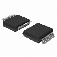
74LV4799DB,118 NXP Semiconductors, 74LV4799DB,118 Datasheet - Page 11

74LV4799DB,118
Manufacturer Part Number
74LV4799DB,118
Description
IC TIMER NICD/NIMH CHRGR 16SSOP
Manufacturer
NXP Semiconductors
Type
Timer Controlr
Series
74LVr
Datasheet
1.74LV4799SD118.pdf
(18 pages)
Specifications of 74LV4799DB,118
Package / Case
16-SSOP
Frequency
100kHz
Voltage - Supply
0.9 V ~ 6 V
Current - Supply
36µA
Operating Temperature
0°C ~ 70°C
Supply Voltage (max)
6 V
Supply Voltage (min)
0.9 V
Maximum Operating Temperature
+ 70 C
Minimum Operating Temperature
0 C
Mounting Style
SMD/SMT
Lead Free Status / RoHS Status
Lead free / RoHS Compliant
Count
-
Lead Free Status / RoHS Status
Lead free / RoHS Compliant, Lead free / RoHS Compliant
Other names
74LV4799DB-T
74LV4799DB-T
935175040118
74LV4799DB-T
935175040118
Philips Semiconductors
Error free operation, even under extreme conditions.
Several measures are taken in the circuit design to ensure
error–free operation, even with very low supply voltages. Moreover,
the circuit has been made very insensitive to the effects of external
fields. The measures taken during the design are:
Synchronous logic and bistable POR.
Use of synchronous logic results in much lower sensitivity to spikes
on input pins. The POR is adapted to fit well into a synchronous
environment. An increasing supply voltage sets the POR. The POR
output signal is routed to the control logic and divider/counter. it is
synchronized with the on–chip clock. After all flip–flops are reset, a
reset acknowledge signal is generated which resets the POR. This
method ensures that the POR signal is acknowledged in all cases,
even at very low voltages.
Data retention.
The circuit may be used in an application where an electric motor is
present. When the motor is switched on, it will disturb the supply
voltage for a short period. The POR level is set at such a level that,
even with very low supply voltages, the POR will not respond during
motor switch on. The flip–flops will retain their data during the supply
voltage disturbance because of the inherent data retention of any
CMOS gate. However, when the battery is almost completely
discharged and the motor switch is activated, the dip on the supply
voltage line can be too large. The retention of the POR is therefore
made deliberately worse than that of the internal flip–fops. The POR
will therefore respond long before the flip–flops will loose their data.
This results in a proper start condition for a new charge cycle.
Debounce circuitry on DIS input.
A discharge cycle is activated by a switch. To protect the circuit from
any bounce of the switch contacts, de–bounce circuitry is provided
1998 Apr 20
Use of synchronous logic
Bistable POR instead of monostable POR
Data retention assured below a supply voltage of 0.9 V.
Debounce circuitry on DIS input (maximum expected debounce
time = 10 ms)
Schmitt trigger on PWRS (power sense) input and on DIS input
Special oscillator security to prevent any malfunction.
Timer for NiCd and NiMH chargers
mains
AC
220 V
110 V
BYD13D
BYD13D
BZD23
BZD23
BYD13D
BYD13D
Figure 2. Typical application of the low-voltage 74LV4799.
BC557
14
15
1
5
7
LED
PWRS
SEL
SCAN
SCI
R C
V in
10
4
11
R D
11
74LV4799
at the DIS input. The circuitry allows a switch de–bounce time of
max. 10 ms.
Schmitt trigger on PWRS (power sense) input.
The PWRS input can be corrupted by high transients due to
disturbances on the mains supply. To suppress any false triggering,
the PWRS input is provided with a Schmitt–trigger. However, for
some applications, it is advisable to connect a low–value capacitor
(150 pF min.) between the PWRS input and GND.
Special oscillator security to prevent any malfunction.
The excellent performance of the oscillator is achieved by using
linear op–amp techniques. The oscillator consists of an internal
reference, two comparators and a latch. Care was taken to design a
very reliable oscillator even with a supply voltage below 0.9 V. If one
of the comparators ceases to operate with a supply voltage below
0.9 V, the latch will not be corrupted. Priority was given to stop the
oscillator rather than allow uncontrolled oscillation.
All these measures result in reliable 1-cell to 4-cell battery charge
management.
Remaining energy indication:
The scan test facility can be used as a remaining energy indication
because the value of the counter can be read–out at the scan output
(MOLLI/SCO). This is achieved by briefly interrupting the normal
mode of operation, putting the circuit in the scan mode
(pin 14 = HIGH), and reading–out of the counter value. The circuit is
then returned to the normal mode (pin 14 = LOW or open).
Read–out procedure: The contents of the counter flip–flops can be
read–out in the scan mode. To ensure that there is no disturbance of
the circuit function, it is essential to either create a round coupled loop
by linking the MOLLI/SCO output (pin 6) directly to the SCI input
pin 15), or to shift–in the serial data of the scan line at the SCI input
after completion of the read out cycle. 49 clock pulses are needed on
the Iosc input (pin 13) to shift–out the contents of the whole scan line.
The most–significant bit of the counter will appear at the MOLLI/SCO
output after the last clock pulse. The least–significant bit after the
penultimate clock pulse, etc. Selecting the last three or four bits will
yield sufficiently high accuracy to obtain the counter value which
represents the remaining energy of the battery.
R S
12
I OSC
13
MOLLI
n.c.
EN
V CC
DIS
3
EN
8
BC327/
BC636
BC547
2
16
6
9
R Z
BC557
buzzer
Product specification
74LV4799
LOAD
battery
SV01647


