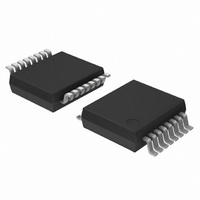
74LV4799DB,118 NXP Semiconductors, 74LV4799DB,118 Datasheet - Page 5

74LV4799DB,118
Manufacturer Part Number
74LV4799DB,118
Description
IC TIMER NICD/NIMH CHRGR 16SSOP
Manufacturer
NXP Semiconductors
Type
Timer Controlr
Series
74LVr
Datasheet
1.74LV4799SD118.pdf
(18 pages)
Specifications of 74LV4799DB,118
Package / Case
16-SSOP
Frequency
100kHz
Voltage - Supply
0.9 V ~ 6 V
Current - Supply
36µA
Operating Temperature
0°C ~ 70°C
Supply Voltage (max)
6 V
Supply Voltage (min)
0.9 V
Maximum Operating Temperature
+ 70 C
Minimum Operating Temperature
0 C
Mounting Style
SMD/SMT
Lead Free Status / RoHS Status
Lead free / RoHS Compliant
Count
-
Lead Free Status / RoHS Status
Lead free / RoHS Compliant, Lead free / RoHS Compliant
Other names
74LV4799DB-T
74LV4799DB-T
935175040118
74LV4799DB-T
935175040118
Philips Semiconductors
Self-discharge mode.
If DIS is HIGH and PWRS is inactive (LOW or open), the battery is
being neither charged nor discharged. The circuit is in the
self-discharge mode. This mode represents the battery leakage
(self-discharge). The counter counts down. The clock frequency is
determined by the external capacitor and resistor at the R
When the counter reaches the zero state, it stops.
LED mode select.
The LED output drives a battery status LED which indicates the
charge/full status of the battery. For optimum flexibility, two modes of
operation are built-in.
NOTE: The blink frequency depends on the oscillator frequency.
Low indication.
As part of the user interface, the MOLLI output shows when the
battery needs to be charged. MOLLI stands for More Or Less Low
Indication (active LOW). The function is as follows: In the discharge
mode, (DIS is active LOW), the counter counts down and, when it
reaches the zero state, it stops. If DIS is switched HIGH, the MOLLI
output gives an output signal of four periods of about one second,
with a 50% duty cycle. This can be used to activate a buzzer. The
MOLLI output signal of four periods will be interrupted as soon as
PWRS is activated.
Alarm indication.
If an almost completely discharged battery is connected to the
charger, it may not be noticed by the user if the load switch is still
FUNCTION TABLE 1
1998 Apr 20
Charge
Trickle charge
Charge/discharge
Discharge
Self-discharge
Mode 1: If SEL is LOW, the LED output is active LOW in the
Mode 2: If SEL is HIGH or open, the LED output blinks with a
Timer for NiCd and NiMH chargers
OPERATING
OPERATING
MODES
(See application information)
charge mode, and the LED blinks with a frequency of
about 1 Hz during trickle charge.
frequency of about 0.25 Hz in the charge mode, and is
active LOW during trickle charge. In the discharge or
self-discharge mode, the LED output is open except
when PWRS is active (HIGH or pulsed). Then, the
battery is charging and discharging simultaneously.
Although the discharge mode is dominant, the LED
output is active when PWRS is also active.
L or open
L or open
H or
H or
H or
PWRS
INPUTS
V
H
H
H
X
X
IN
DIS
H
H
H
L
L
S
output.
EN
H
H
L
L
EN
Z
Z
L
L
5
OUTPUTS
on. To prevent damaging the battery, an alarm signal on the LED
output will alert the user to switch off the load. The alarm signal is
easily recognized, because the LED output will blink at a higher
frequency than normal (about 5 Hz instead of 1 Hz). This alarm
indication is only active if the SEL input is HIGH or open. If the SEL
input is LOW, no alarm indication is present, because in many
applications simultaneous charging and discharging is quite
acceptable. (See charge/discharge mode)
Scan test mode.
If the SCAN input (pin 14) is made active HIGH, the circuit is in the
test mode. The tester clock is connected to the I
the scan mode, the on–chip oscillator is bypassed to allow rapid
testing of the divider/counter. The scan test patterns are available on
request. The scan test data is entered serially through the SCI input
(pin 15). The scan out data is present on the MOLLI/SCO output
(pin 6), which then acts as a scan output.
Remaining energy indication.
The scan test facility can be used as a remaining energy indication
because the value of the counter can be read out at the scan output
(MOLLI/SCO). This is done by briefly interrupting the normal mode
of operation, putting the circuit in the scan mode, and reading out
the counter value. The circuit then reverts to the normal mode. This
only works correctly with the MOLLI/SCO output and SCI input
linked (round coupled loop) and with exactly 49 clock pulses applied
to the I
The serial scan-out data is available on the MOLLI/SCO output. The
value of the counter can be decoded by reading the correct bits.
Details are given later in the section “Application information”.
Output drivers EN and EN.
In one-cell battery (low-voltage) applications, the drive from the
ENABLE output (EN) is insufficient to provide the base current directly
for the external bipolar PNP regulator transistor. The inverse signal has
therefore been made available at the ENABLE output (EN) to drive an
extra bipolar NPN transistor that can provide the base current for the
bipolar PNP regulator transistor as shown in Figure 2.
R
Z
Z
Z
C
OSC
R
Z
Z
Z
input.
D
R
Z
Z
Z
S
Count up 22 sections
Stop
Count down 18 sections
Count down 18 sections
Count down 27 sections
MODE
DIVIDER/COUNTER
Product specification
74LV4799
OSC
pin (pin 13). In
VALUE
max
max
min
min
min


