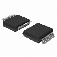
74LV4799DB,118 NXP Semiconductors, 74LV4799DB,118 Datasheet - Page 7

74LV4799DB,118
Manufacturer Part Number
74LV4799DB,118
Description
IC TIMER NICD/NIMH CHRGR 16SSOP
Manufacturer
NXP Semiconductors
Type
Timer Controlr
Series
74LVr
Datasheet
1.74LV4799SD118.pdf
(18 pages)
Specifications of 74LV4799DB,118
Package / Case
16-SSOP
Frequency
100kHz
Voltage - Supply
0.9 V ~ 6 V
Current - Supply
36µA
Operating Temperature
0°C ~ 70°C
Supply Voltage (max)
6 V
Supply Voltage (min)
0.9 V
Maximum Operating Temperature
+ 70 C
Minimum Operating Temperature
0 C
Mounting Style
SMD/SMT
Lead Free Status / RoHS Status
Lead free / RoHS Compliant
Count
-
Lead Free Status / RoHS Status
Lead free / RoHS Compliant, Lead free / RoHS Compliant
Other names
74LV4799DB-T
74LV4799DB-T
935175040118
74LV4799DB-T
935175040118
1. Single sided input protection applied on pins 4, 5, and 9.
1. In applications where a motor is present, the input voltage may exceed the maximum V
2. Stresses beyond those listed may cause permanent damage to the device. These are stress ratings only and functional operation of the
3. The input and output voltage ratings may be exceeded if the input and output current ratings are observed.
Philips Semiconductors
RECOMMENDED OPERATING CONDITIONS
NOTE:
ABSOLUTE MAXIMUM RATINGS
In accordance with the Absolute Maximum Rating System (IEC 134).
Voltages are referenced to GND (ground = 0 V).
NOTES:
1998 Apr 20
SYMBOL
SYMBOL
I
GND
Timer for NiCd and NiMH chargers
when the motor is switched off.
device at these or any other conditions beyond those under “recommended operating conditions” is not implied. Exposure to absolute
maximum rated conditions for extended periods may affect device reliability.
T
V
t
V
V
T
amb
r
I
I
P
P
V
CC
, t
I
V
V
OK
I
OK
I
CC
IK
stg
O
O
O
t t
tot
I
, I
I
I
f
CC
DC supply voltage
Input voltage pins 4, 5, and 9
Input voltage pins 7, 13, 14, and 15
Output voltage pins 10, 11, and 12
Output voltage pins 1, 2, 3, and 6
Operating ambient temperature range in free air
Input rise and fall times pin 5
Input rise and fall times pins 7, 14 and 15
Input rise and fall times pin 9
DC supply voltage
DC input diode current pins 4, 5 and 9
DC input diode current pins 7, 13, 14 and 15
NON repetitive peak DC input diode current pin 9
DC input voltage range pins 4, 5 and 9
DC input voltage range pins 7, 13, 14 and 15
DC output diode current pins 1, 2, 3 and 6
DC output sink current pins 1, 2, 3 and 6
DC output diode current pins 10, 11 and 12
DC output sink or source current pins 10, 11 and 12
DC GND or V
Storage temperature range
Power dissipation per package
Power dissi ation er ackage
Plastic DIL
Plastic mini-pack (SO)
Pl
Plastic shrink mini-pack (SSOP and TSSOP)
ti
h i k
CC
i i
PARAMETER
current
PARAMETER
k (SSOP
2, 3
d TSSOP)
characteristics per device
V
V
V
V
V
V
V
V
V
V
–0.5 V
for temperature range: –40 to +125 C
for tem erature range: 40 to +125 C
above + 70 C derate linearly with 12 mW/K
above + 70 C derate linearly with 8 mW/K
above + 60 C derate linearly with 5.5 mW/K
CC
CC
CC
CC
b
I
I
I
O
O
O
See DC and AC
7
CONDITIONS
= 3.6V; V
= 1.0V; V
= 2.0V; V
= 3.0V; V
See Note 1
10 V and t
–0.5 or V
–0.5 or V
–0.5 V
0 V
–0.5 or V
60 C d
V
O
I
I
I
I
I
I
= 6.0V
V
= 1.0V
= 2.0V
= 4.5V
O
CONDITIONS
CC
12 V
V
10 ms; see note 1
CC
V
+ 0.5 V
t li
CC
+ 0.5 V
I
, level of 10 V at the DIS input for a very short period
+ 0.5 V
l
y
MIN
0.9
0
0
0
0
0
–
–
–
–
–
–
ith 5 5
W/K
TYP
1.2
–
–
–
–
–
–
–
–
–
–
–0.5
–0.5
–0.5
MIN
–65
MAX
V
V
+70
Product specification
74LV4799
500
200
100
10
10
10
50
V
6
2
CC
CC
CC
MAX
+150
+7.0
+20
+12
–20
–25
750
500
400
400
10
20
20
25
50
+ 0.5
UNIT
ms
ns
V
V
V
UNIT
C
mW
mW
s
mA
mA
mA
mA
mA
mA
V
V
V
C


