ISL12026IBZ Intersil, ISL12026IBZ Datasheet - Page 2
ISL12026IBZ
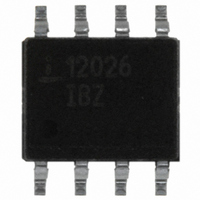
Manufacturer Part Number
ISL12026IBZ
Description
IC RTC/CALENDAR EEPROM 8-SOIC
Manufacturer
Intersil
Type
Clock/Calendar/EEPROMr
Specifications of ISL12026IBZ
Memory Size
4K (512 x 8)
Time Format
HH:MM:SS (12/24 hr)
Date Format
YY-MM-DD-dd
Interface
I²C, 2-Wire Serial
Voltage - Supply
2.7 V ~ 5.5 V
Operating Temperature
-40°C ~ 85°C
Mounting Type
Surface Mount
Package / Case
8-SOIC (3.9mm Width)
Clock Format
HH
Clock Ic Type
RTC
Interface Type
I2C, Serial
Memory Configuration
512 X 8
Supply Voltage Range
2.7V To 5.5V
Digital Ic Case Style
SOIC
Rohs Compliant
Yes
Lead Free Status / RoHS Status
Lead free / RoHS Compliant
Available stocks
Company
Part Number
Manufacturer
Quantity
Price
Company:

Part Number:
ISL12026IBZ
Manufacturer:
INTELSEL
Quantity:
60
Part Number:
ISL12026IBZ
Manufacturer:
INTERSIL
Quantity:
20 000
Part Number:
ISL12026IBZ-T
Manufacturer:
INTERSIL
Quantity:
20 000


Ordering Information
NOTES:
Block Diagram
Pin Descriptions
ISL12026IBZ
ISL12026IVZ
ISL12026AIBZ
ISL12026AIVZ
1. Add “-T*” suffix for tape and reel. Please refer to
2. These Intersil Pb-free plastic packaged products employ special Pb-free material sets, molding compounds/die attach materials, and 100% matte
3. For Moisture Sensitivity Level (MSL), please see device information page for
IRQ/F
SOIC
tin plate plus anneal (e3 termination finish, which is RoHS compliant and compatible with both SnPb and Pb-free soldering operations). Intersil Pb-
free products are MSL classified at Pb-free peak reflow temperatures that meet or exceed the Pb-free requirements of IPC/JEDEC J STD-020.
techbrief TB363.
PIN NUMBER
1
2
3
4
5
6
7
8
SCL
SDA
OUT
PART NUMBER
(Notes 1, 2, 3)
32.768kHz
TSSOP
INTERFACE
DECODER
SERIAL
3
4
5
6
7
8
1
2
SELECT
X1
X2
IRQ/F
SYMBOL
CONTROL
V
DECODE
GND
SDA
SCL
V
8
LOGIC
X1
X2
BAT
12026 IBZ
2026 IVZ
12026A IBZ
2026A IVZ
DD
OUT
2
MARKING
PART
The X1 pin is the input of an inverting amplifier and is intended to be connected to one pin of an external
32.768kHz quartz crystal. X1 can also be driven directly from a 32.768kHz source (see “Application Section”
on page 19.)
The X2 pin is the output of an inverting amplifier and is intended to be connected to one pin of an external
32.768kHz quartz crystal (see “Application Section” on page 19.)
Interrupt Output/Frequency Output is a multi-functional pin that can be used as interrupt or frequency
output pin. The function is set via the control register. This output is an open drain configuration.
Ground.
Serial Data (SDA) is a bidirectional pin used to transfer serial data into and out of the device. It has an open
drain output and may be wire OR’ed with other open drain or open collector outputs.
The Serial Clock (SCL) input is used to clock all serial data into and out of the device. The input buffer on
this pin is always active (not gated).
This input provides a backup supply voltage to the device. V
that the V
Power Supply.
REGISTERS
CONTROL/
(EEPROM)
OSCILLATOR
COMPENSATION
DD
V
BAT
TB347
supply fails. This pin should be tied to ground if not used.
V
V
ISL12026, ISL12026A
DD
DD
OSC
TRIP POINT
(V)
2.2
2.2
< V
< V
for details on reel specifications.
BAT
BAT
REGISTERS
FREQUENCY
STATUS
(SRAM)
DIVIDER
BSW BIT DEFAULT
1Hz
SETTING
BSW = 1
BSW = 1
BSW = 0
BSW = 0
ISL12026,
CALENDAR
ALARM
TIMER
LOGIC
DESCRIPTION
ISL12026A. For more information on MSL please see
TEMP RANGE
ALARM REGS
REGISTERS
-40 to +85
-40 to +85
-40 to +85
-40 to +85
COMPARE
EEPROM
(EEPROM)
KEEPING
ARRAY
(SRAM)
BAT
(°C)
TIME
4k
supplies power to the device in the event
8 Ld SOIC
8 Ld TSSOP
8 Ld SOIC
8 Ld TSSOP
PACKAGE
(Pb-Free)
CIRCUITRY
BATTERY
SWITCH
M8.15
M8.173
M8.15
M8.173
November 30, 2010
DWG. #
PKG.
V
V
DD
BAT
FN8231.9
Related parts for ISL12026IBZ
Image
Part Number
Description
Manufacturer
Datasheet
Request
R

Part Number:
Description:
Intersil Corporation [CMOS Serial Controller Interface]
Manufacturer:
Intersil Corporation
Datasheet:
Part Number:
Description:
Manufacturer:
Intersil Corporation
Datasheet:
Part Number:
Description:
357-036-542-201 CARDEDGE 36POS DL .156 BLK LOPRO
Manufacturer:
Intersil Corporation
Datasheet:
Part Number:
Description:
1024-Word x 4-Bit LSI Static RAM
Manufacturer:
Intersil Corporation
Datasheet:
Part Number:
Description:
General Purpose NPN Transistor Arrays FN341.4
Manufacturer:
Intersil Corporation
Datasheet:
Part Number:
Description:
CMOS 16-Bit Microprocessor
Manufacturer:
Intersil Corporation
Datasheet:
Part Number:
Description:
Manufacturer:
Intersil Corporation
Datasheet:
Part Number:
Description:
Manufacturer:
Intersil Corporation
Datasheet:
Part Number:
Description:
Manufacturer:
Intersil Corporation
Datasheet:
Part Number:
Description:
Manufacturer:
Intersil Corporation
Datasheet:
Part Number:
Description:
CMOS 6-Bit Latch and Decoder Memory Interfaces
Manufacturer:
Intersil Corporation
Datasheet:
Part Number:
Description:
CA3046General Purpose NPN Transistor Arrays
Manufacturer:
Intersil Corporation
Datasheet:
Part Number:
Description:
Manufacturer:
Intersil Corporation
Datasheet:
Part Number:
Description:
TR909 DLC/FLC SLIC with Low Power Standby
Manufacturer:
Intersil Corporation
Datasheet:
Part Number:
Description:
Manufacturer:
Intersil Corporation
Datasheet: