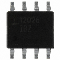
ISL12026IBZ Intersil, ISL12026IBZ Datasheet - Page 20

ISL12026IBZ
Manufacturer Part Number
ISL12026IBZ
Description
IC RTC/CALENDAR EEPROM 8-SOIC
Manufacturer
Intersil
Type
Clock/Calendar/EEPROMr
Specifications of ISL12026IBZ
Memory Size
4K (512 x 8)
Time Format
HH:MM:SS (12/24 hr)
Date Format
YY-MM-DD-dd
Interface
I²C, 2-Wire Serial
Voltage - Supply
2.7 V ~ 5.5 V
Operating Temperature
-40°C ~ 85°C
Mounting Type
Surface Mount
Package / Case
8-SOIC (3.9mm Width)
Clock Format
HH
Clock Ic Type
RTC
Interface Type
I2C, Serial
Memory Configuration
512 X 8
Supply Voltage Range
2.7V To 5.5V
Digital Ic Case Style
SOIC
Rohs Compliant
Yes
Lead Free Status / RoHS Status
Lead free / RoHS Compliant
Available stocks
Company
Part Number
Manufacturer
Quantity
Price
Company:
Part Number:
ISL12026IBZ
Manufacturer:
INTELSEL
Quantity:
60
Part Number:
ISL12026IBZ
Manufacturer:
INTERSIL
Quantity:
20 000
Part Number:
ISL12026IBZ-T
Manufacturer:
INTERSIL
Quantity:
20 000
Citizen
Epson
Raltron
SaRonix
Ecliptek
ECS
Fox
MANUFACTURER
The turnover temperature in Table 7 describes the
temperature where the apex of the of the drift vs temperature
curve occurs. This curve is parabolic with the drift increasing
as (T - T0)
turnover temperature is typically +25°C, and a peak drift of
>110ppm occurs at the temperature extremes of -40°C and
+85°C. It is possible to address this variable drift by adjusting
the load capacitance of the crystal, which will result in
predictable change to the crystal frequency. The Intersil RTC
family allows this adjustment over temperature since the
devices include on-chip load capacitor trimming. This control
is handled by the Analog Trimming Register, or ATR, which
has 6-bits of control. The load capacitance range covered by
the ATR circuit is approximately 3.25pF to 18.75pF, in
0.25pF increments. Note that actual capacitance would also
include about 2pF of package related capacitance. In-circuit
tests with commercially available crystals demonstrate that
this range of capacitance allows frequency control from
+80ppm to -34ppm, using a 12.5pF load crystal.
In addition to the analog compensation afforded by the
adjustable load capacitance, a digital compensation feature
is available for the Intersil RTC family. There are 3-bits
known as the Digital Trimming Register or DTR, and they
operate by adding or skipping pulses in the clock signal. The
range provided is ±30ppm in increments of 10ppm. The
default setting is 0ppm. The DTR control can be used for
coarse adjustments of frequency drift over-temperature or
for crystal initial accuracy correction.
A final application for the ATR control is in-circuit calibration
for high accuracy applications, along with a temperature
sensor chip. Once the RTC circuit is powered up with battery
backup, the IRQ/F
frequency drift is measured. The ATR control is then
adjusted to a setting which minimizes drift. Once adjusted at
a particular temperature, it is possible to adjust at other
discrete temperatures for minimal overall drift, and store the
resulting settings in the EEPROM. Extremely low overall
temperature drift is possible with this method. The Intersil
evaluation board contains the circuitry necessary to
implement this control.
2
TABLE 8. CRYSTAL MANUFACTURERS
. For an Epson MC-405 device, for example, the
CM201, CM202, CM200S -40 to +85
MC-405, MC-406
RSM-200S-A or B
32S12A or B
ECPSM29T-32.768K
ECX-306/ECX-306I
FSM-327
OUT
NUMBER
output is set at 32.768kHz and
PART
20
-40 to +85
-40 to +85
-40 to +85
-10 to +60
-10 to +60
-40 to +85
RANGE
TEMP
(°C)
ISL12026, ISL12026A
+25°C FREQ.
TOLERANCE
±20ppm
±20ppm
±20ppm
±20ppm
±20ppm
±20ppm
±20ppm
(ppm)
Layout Considerations
The crystal input at X1 has a very high impedance and will
pick up high frequency signals from other circuits on the
board. Since the X2 pin is tied to the other side of the crystal,
it is also a sensitive node. These signals can couple into the
oscillator circuit and produce double clocking or
mis-clocking, seriously affecting the accuracy of the RTC.
Care needs to be taken in layout of the RTC circuit to avoid
noise pickup. In Figure 23 is a suggested layout for the
ISL12026 or ISL12027 devices in 8 Ld SO package.
The X1 and X2 connections to the crystal are to be kept as
short as possible. A thick ground trace around the crystal is
advised to minimize noise intrusion, but ground near the X1
and X2 pins should be avoided as it will add to the load
capacitance at those pins. Keep in mind these guidelines for
other PCB layers in the vicinity of the RTC device. A small
decoupling capacitor at the V
with a solid connection to ground.
The ISL12026 product has a special consideration. The
IRQ/F
the X2 pin. When this pin is used as a frequency output
(IRQ/F
X1 or X2 pins and cause double-clocking. The layout in
Figure 23 minimizes this by running the IRQ/F
away from the X1 and X2 pins. Also, reducing the switching
current at this pin by careful selection of the pull-up resistor
value will reduce noise. Intersil suggests a minimum value of
5.1kΩ for 32.768kHz, and higher values (up to 20kΩ) for
lower frequency IRQ/F
For other RTC products, the same rules previously stated
should be observed, but slightly adjusted since the
packages and pinouts are different.
Oscillator Measurements
When a proper crystal is selected and the layout guidelines
above are observed, the oscillator should start-up in most
FIGURE 23. SUGGESTED LAYOUT FOR INTERSIL RTC IN SO-8
OUT
OUT
- pin on the 8 Ld SOIC package is located next to
) and is set to 32.768kHz, noise can couple to the
OUT
X1
outputs.
DD
pin of the chip is mandatory,
U1
OUT
November 30, 2010
R5
47k
output
FN8231.9


