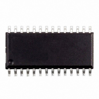
M41ST85YMH6E STMicroelectronics, M41ST85YMH6E Datasheet - Page 10

M41ST85YMH6E
Manufacturer Part Number
M41ST85YMH6E
Description
IC RTC 5.0V 512BIT NVRAM 28SOIC
Manufacturer
STMicroelectronics
Type
Clock/Calendar/Supervisorr
Datasheet
1.M41ST85YMH6E.pdf
(34 pages)
Specifications of M41ST85YMH6E
Memory Size
64B
Time Format
HH:MM:SS:hh (24 hr)
Date Format
YY-MM-DD-dd
Interface
I²C, 2-Wire Serial
Voltage - Supply
4.5 V ~ 5.5 V
Operating Temperature
-40°C ~ 85°C
Mounting Type
Surface Mount
Package / Case
28-SOIC, 28-SOH (8.48mm Width)
Lead Free Status / RoHS Status
Contains lead / RoHS non-compliant
Other names
497-2806-5
M41ST85YMH6
M41ST85YMH6
Available stocks
Company
Part Number
Manufacturer
Quantity
Price
Company:
Part Number:
M41ST85YMH6E
Manufacturer:
IR
Quantity:
5 000
M41ST85Y, M41ST85W
READ Mode
In this mode the master reads the M41ST85Y/W
slave after setting the slave address (see
11., page
Bit (R/W=0) and the Acknowledge Bit, the word
address 'An' is written to the on-chip address
pointer. Next the START condition and slave ad-
dress are repeated followed by the READ Mode
Control Bit (R/W=1). At this point the master trans-
mitter becomes the master receiver.
The data byte which was addressed will be trans-
mitted and the master receiver will send an Ac-
knowledge Bit to the slave transmitter. The
address pointer is only incremented on reception
of an Acknowledge Clock. The M41ST85Y/W
slave transmitter will now place the data byte at
address An+1 on the bus, the master receiver
reads and acknowledges the new byte and the ad-
dress pointer is incremented to An+2.
Figure 11. Slave Address Location
Figure 12. READ Mode Sequence
10/34
BUS ACTIVITY:
MASTER
SDA LINE
BUS ACTIVITY:
10). Following the WRITE Mode Control
S
ADDRESS
SLAVE
DATA n+X
START
ADDRESS (An)
WORD
P
1
Figure
1
SLAVE ADDRESS
S
0
ADDRESS
SLAVE
1
This cycle of reading consecutive addresses will
continue until the master receiver sends a STOP
condition to the slave transmitter (see
12., page
The system-to-user transfer of clock data will be
halted whenever the address being read is a clock
address (00h to 07h). The update will resume ei-
ther due to a Stop Condition or when the pointer
increments to a non-clock or RAM address.
Note: This is true both in READ Mode and WRITE
Mode.
An alternate READ Mode may also be implement-
ed whereby the master reads the M41ST85Y/W
slave without first writing to the (volatile) address
pointer. The first address that is read is the last
one
13., page
0
0
stored
0
R/W
10).
11).
DATA n
A
in
AI00602
the
DATA n+1
pointer
AI00899
(see
Figure
Figure


