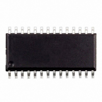
M41ST85YMH6E STMicroelectronics, M41ST85YMH6E Datasheet - Page 12

M41ST85YMH6E
Manufacturer Part Number
M41ST85YMH6E
Description
IC RTC 5.0V 512BIT NVRAM 28SOIC
Manufacturer
STMicroelectronics
Type
Clock/Calendar/Supervisorr
Datasheet
1.M41ST85YMH6E.pdf
(34 pages)
Specifications of M41ST85YMH6E
Memory Size
64B
Time Format
HH:MM:SS:hh (24 hr)
Date Format
YY-MM-DD-dd
Interface
I²C, 2-Wire Serial
Voltage - Supply
4.5 V ~ 5.5 V
Operating Temperature
-40°C ~ 85°C
Mounting Type
Surface Mount
Package / Case
28-SOIC, 28-SOH (8.48mm Width)
Lead Free Status / RoHS Status
Contains lead / RoHS non-compliant
Other names
497-2806-5
M41ST85YMH6
M41ST85YMH6
Available stocks
Company
Part Number
Manufacturer
Quantity
Price
Company:
Part Number:
M41ST85YMH6E
Manufacturer:
IR
Quantity:
5 000
M41ST85Y, M41ST85W
Data Retention Mode
With valid V
accessed as described above with READ or
WRITE Cycles. Should the supply voltage decay,
the M41ST85Y/W will automatically deselect,
write protecting itself (and any external SRAM)
when
V
hibiting access to the clock registers. At this time,
the Reset pin (RST) is driven active and will re-
main active until V
ternal RAM access is inhibited in a similar manner
by forcing E
0.2 volts of the V
as long as V
dition. When V
Switchover Voltage (V
from the V
the clock registers and external SRAM are main-
tained from the attached battery supply.
All outputs become high impedance. The V
is capable of supplying 100 µA of current to the at-
tached memory with less than 0.3 volts drop under
this condition. On power up, when V
a nominal value, write protection continues for t
by inhibiting E
active during this time (see
Note: Most low power SRAMs on the market to-
day can be used with the M41ST85Y/W RTC SU-
PERVISOR. There are, however some criteria
which should be used in making the final choice of
12/34
PFD
(min). This is accomplished by internally in-
V
CC
CC
CON
CC
CC
pin to the SNAPHAT
CON
falls
CC
remains at an out-of-tolerance con-
applied, the M41ST85Y/W can be
to a high level. This level is within
BAT
CC
falls below the Battery Back-up
. The RST signal also remains
. E
returns to nominal levels. Ex-
between
SO
CON
), power input is switched
will remain at this level
Figure 22., page
V
PFD
®
CC
(max)
battery, and
returns to
OUT
27).
and
pin
rec
an SRAM to use. The SRAM must be designed in
a way where the chip enable input disables all oth-
er inputs to the SRAM. This allows inputs to the
M41ST85Y/W and SRAMs to be “Don’t Care”
once V
should also guarantee data retention down to
V
be sufficient to meet the system needs with the
chip enable output propagation delays included. If
the SRAM includes a second chip enable pin (E2),
this pin should be tied to V
If data retention lifetime is a critical parameter for
the system, it is important to review the data reten-
tion current specifications for the particular
SRAMs being evaluated. Most SRAMs specify a
data retention current at 3.0 volts. Manufacturers
generally specify a typical condition for room tem-
perature along with a worst case condition (gener-
ally at elevated temperatures). The system level
requirements will determine the choice of which
value to use. The data retention current value of
the SRAMs can then be added to the I
the M41ST85Y/W to determine the total current re-
quirements for data retention. The available bat-
tery capacity for the SNAPHAT
can then be divided by this current to determine
the amount of data retention available (see
19., page
For a further more detailed review of lifetime calcu-
lations, please see Application Note AN1012.
CC
=2.0 volts. The chip enable access time must
CC
32).
falls below V
OUT
PFD
(min). The SRAM
.
®
of your choice
BAT
value of
Table


