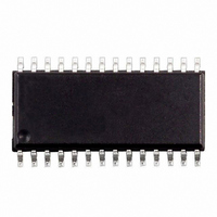
M41ST85YMH6E STMicroelectronics, M41ST85YMH6E Datasheet - Page 11

M41ST85YMH6E
Manufacturer Part Number
M41ST85YMH6E
Description
IC RTC 5.0V 512BIT NVRAM 28SOIC
Manufacturer
STMicroelectronics
Type
Clock/Calendar/Supervisorr
Datasheet
1.M41ST85YMH6E.pdf
(34 pages)
Specifications of M41ST85YMH6E
Memory Size
64B
Time Format
HH:MM:SS:hh (24 hr)
Date Format
YY-MM-DD-dd
Interface
I²C, 2-Wire Serial
Voltage - Supply
4.5 V ~ 5.5 V
Operating Temperature
-40°C ~ 85°C
Mounting Type
Surface Mount
Package / Case
28-SOIC, 28-SOH (8.48mm Width)
Lead Free Status / RoHS Status
Contains lead / RoHS non-compliant
Other names
497-2806-5
M41ST85YMH6
M41ST85YMH6
Available stocks
Company
Part Number
Manufacturer
Quantity
Price
Company:
Part Number:
M41ST85YMH6E
Manufacturer:
IR
Quantity:
5 000
Figure 13. Alternate READ Mode Sequence
WRITE Mode
In this mode the master transmitter transmits to
the M41ST85Y/W slave receiver. Bus protocol is
shown in
START condition and slave address, a logic '0' (R/
W=0) is placed on the bus and indicates to the ad-
dressed device that word address An will follow
and is to be written to the on-chip address pointer.
The data word to be written to the memory is
Figure 14. WRITE Mode Sequence
BUS ACTIVITY:
MASTER
SDA LINE
BUS ACTIVITY:
Figure 14., page
BUS ACTIVITY:
MASTER
SDA LINE
BUS ACTIVITY:
S
ADDRESS
SLAVE
S
ADDRESS
SLAVE
11. Following the
ADDRESS (An)
WORD
DATA n
strobed in next and the internal address pointer is
incremented to the next memory location within
the RAM on the reception of an acknowledge
clock. The M41ST85Y/W slave receiver will send
an acknowledge clock to the master transmitter af-
ter it has received the slave address (see
11., page
word address and each data byte.
DATA n
DATA n+1
10) and again after it has received the
DATA n+1
M41ST85Y, M41ST85W
DATA n+X
DATA n+X
AI00895
AI00591
P
P
Figure
11/34


