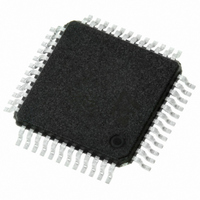
STLC7550TQF7TR STMicroelectronics, STLC7550TQF7TR Datasheet - Page 12

STLC7550TQF7TR
Manufacturer Part Number
STLC7550TQF7TR
Description
IC ANALOG FRONT END LV 48-TQFP
Manufacturer
STMicroelectronics
Datasheet
1.E-STLC7550TQF7.pdf
(24 pages)
Specifications of STLC7550TQF7TR
Number Of Bits
16
Number Of Channels
1
Power (watts)
30mW
Voltage - Supply, Analog
3V
Voltage - Supply, Digital
3V
Package / Case
48-TQFP, 48-VQFP
Lead Free Status / RoHS Status
Lead free / RoHS Compliant
Available stocks
Company
Part Number
Manufacturer
Quantity
Price
Company:
Part Number:
STLC7550TQF7TR
Manufacturer:
STMicroelectronics
Quantity:
10 000
Functional description
2.5
12/24
Host interface
Figure 8.
The Host interface consist of the shift clock, the frame synchronization signal, the
ADCchannel data output, and the DAC-channel data input.
Two modes of serial transfer are available :
Both modes are selected by the Hardware Control pins (HC0, HC1).
The data to the device, input/output are MSB-first in 2’s complement format (see
When Control Mode is selected, the device will internally generate an additional Frame
Synchronization Pulse (Secondary Frame Synchronization Pulse) at the midpoint of the
original Frame Period. If the device is in slave mode the additional frame sync (secondary
frame sync pulse) must be generated by the processor. The Original Frame Synchronization
Pulse will also be referred to as the Primary Frame Synchronization Pulse.
Table 3.
HC1
0
0
–
–
HC0
First : Software mode for 15-bit transmit data transfer and 16-bit receive data
transfer
Second : hardware mode for 16-bit data transfer.
0
0
Configuration 5
Mode selection
LSB
0
1
15bits (+16bits reg.)
Useful Data
PROCESSOR
15bits
BCLK
DO
FS
DI
V
DD
Rev 9
Secondary
FSYNC
Yes
No
SCLK
FS
DIN
DOUT
XTAKIN
TS
FS
DIN
DOUT
f
HC0
HC0
STLC7550
Q
STLC7550
= 36.864MHz
XTALIN
Software Mode for Data Transfer only.
Software Mode for Data Transfer + Control
Register Transfer.
MCM
HC1
HC1
MCM
M/S
M/S
TS
V
V
GND
GND
GND
DD
DD
Description
STLC7550
Table
3).


