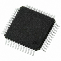
STLC7550TQF7TR STMicroelectronics, STLC7550TQF7TR Datasheet - Page 6

STLC7550TQF7TR
Manufacturer Part Number
STLC7550TQF7TR
Description
IC ANALOG FRONT END LV 48-TQFP
Manufacturer
STMicroelectronics
Datasheet
1.E-STLC7550TQF7.pdf
(24 pages)
Specifications of STLC7550TQF7TR
Number Of Bits
16
Number Of Channels
1
Power (watts)
30mW
Voltage - Supply, Analog
3V
Voltage - Supply, Digital
3V
Package / Case
48-TQFP, 48-VQFP
Lead Free Status / RoHS Status
Lead free / RoHS Compliant
Available stocks
Company
Part Number
Manufacturer
Quantity
Price
Company:
Part Number:
STLC7550TQF7TR
Manufacturer:
STMicroelectronics
Quantity:
10 000
Pins description & Block diagram
1.1.3
1.1.4
6/24
Master/Slave Control (M/S)
When M/S is high, the device is in master mode and Fs is generated internally. When M/S is
low, the device is in slave mode and Fs must be generated externally.
Master Clock Mode (MCM)
When MCM is high, XTALIN is provided externally and must be equal to 36.864MHz. When
MCM is low, XTALIN is provided externally and must be equal to oversampling frequency :
Fs x Over (see
Timeslot Control (TS)
When TS = 0 the data are assigned to the first 16 bits after falling edge of FS (7546 mode)
otherwise the data are bits 17 to 32. The case M/S = 1 with TS = 1 is reserved for life-test
(transmit gain fixed to 0dB).
Clock signals (2 pins)
Depending on MCM value, these pins have different function.
MCM = 1 (XTALIN, XTALOUT)
These pins must be tied to external crystal. For the value of crystal see
MCM = 0 (MCLK, XTALOUT)
MCLK Pin must be connected to an external clock. XTALOUT is not used.
Analog interface (9 pins)
DAC and ADC Positive Reference Voltage Output (V
This pin provides the Positive Reference Voltage used by the 16-bit converters. The
reference voltage, V
and its nominal value is 1.25V. V
DAC and ADC Negative Reference Voltage Output (V
This pin provides the Negative Reference Voltage used by the 16-bit converters, and should
be externally decoupled with respect to V
Common Mode Voltage Output (V
This output pin is the common mode voltage (AV
decoupled with respect to GND.
Non-inverting Smoothing Filter Output(OUT+)
This pin is the non-inverting output of the fully differential analog smoothing filter.
Inverting Smoothing Filter Output (OUT-)
This pin is the inverting output of the fully differential analog smoothing filter. Outputs OUT+
and OUTprovide analog signals with maximum peak-topeak amplitude 2 x VREF, and must
be followed by an external two pole smoothing filter. The external filter follows the internal
single pole switch capacitor filter. The cutoff frequency of the external filter must be greater
Figure 3
REF
, is the voltage difference between the V
and
Section
REFP
2.4).
Rev 9
should be externally decoupled with respect to V
CM
CM
)
.
DD
- AGND)/2. This output must be
REFP
REFN
REFP
)
)
and V
Section
REFN
2.3.
outputs,
STLC7550
CM
.


