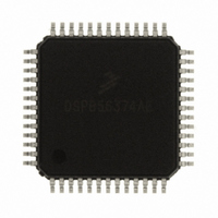
DSPB56374AE Freescale Semiconductor, DSPB56374AE Datasheet - Page 25

DSPB56374AE
Manufacturer Part Number
DSPB56374AE
Description
IC DSP 24BIT 150MHZ 52-LQFP
Manufacturer
Freescale Semiconductor
Series
Symphony™r
Type
Audio Processorr
Datasheet
1.DSPB56374AE.pdf
(64 pages)
Specifications of DSPB56374AE
Interface
Host Interface, I²C, SAI, SPI
Clock Rate
150MHz
Non-volatile Memory
ROM (84 kB)
On-chip Ram
54kB
Voltage - I/o
3.30V
Voltage - Core
1.25V
Operating Temperature
-40°C ~ 110°C
Mounting Type
Surface Mount
Package / Case
52-LQFP
Product
DSPs
Data Bus Width
24 bit
Processor Series
DSP563xx
Core
56000
Numeric And Arithmetic Format
Fixed-Point
Device Million Instructions Per Second
150 MIPS
Maximum Clock Frequency
150 MHz
Program Memory Type
Flash
Program Memory Size
24 KB
Data Ram Size
54 KB
Operating Supply Voltage
1.25 V or 3.3 V
Maximum Operating Temperature
+ 110 C
Mounting Style
SMD/SMT
Interface Type
SIA, SHI
Minimum Operating Temperature
- 40 C
Leaded Process Compatible
Yes
Rohs Compliant
Yes
Peak Reflow Compatible (260 C)
Yes
Lead Free Status / Rohs Status
Lead free / RoHS Compliant
Available stocks
Company
Part Number
Manufacturer
Quantity
Price
Company:
Part Number:
DSPB56374AE
Manufacturer:
DELPHI
Quantity:
10 000
Company:
Part Number:
DSPB56374AE
Manufacturer:
QFP
Quantity:
591
Company:
Part Number:
DSPB56374AE
Manufacturer:
Freescale Semiconductor
Quantity:
10 000
Part Number:
DSPB56374AE
Manufacturer:
FREESCALE
Quantity:
20 000
Company:
Part Number:
DSPB56374AEC
Manufacturer:
Freescale Semiconductor
Quantity:
10 000
4.11 JTAG/OnCE Interface
5
Freescale Semiconductor
Signal
Name
PLOCK
TDO
TMS
TCK
Signal
TDI
Name
Maximum Ratings
This device contains circuitry protecting against damage due to high static voltage
or electrical fields. However, normal precautions should be taken to avoid
exceeding maximum voltage ratings. Reliability of operation is enhanced if unused
inputs are pulled to an appropriate logic voltage level (e.g., either GND or V
The suggested value for a pullup or pulldown resistor is 4.7 kΩ.
Signal
Output
Type
Input
Input
Input
Output
Type
Tri-stated
during
Reset
State
Input
Input
Input
during
Reset
State
Table 13. Timer Signal (continued)
Test Data Input—TDI is a test data serial input signal used for test instructions
Test Clock—TCK is a test clock input signal used to synchronize the JTAG test
logic.
Internal Pull up resistor.
This input is 5 V tolerant.
and data. TDI is sampled on the rising edge of TCK.
Internal Pull up resistor.
This input is 5 V tolerant.
Test Data Output—TDO is a test data serial output signal used for test
instructions and data. TDO is tri-statable and is actively driven in the shift-IR
and shift-DR controller states. TDO changes on the falling edge of TCK.
Test Mode Select—TMS is an input signal used to sequence the test
controller’s state machine. TMS is sampled on the rising edge of TCK.
Internal Pull up resistor.
This input is 5 V tolerant.
Table 14. JTAG/OnCE Interface
DSP56374 Data Sheet, Rev. 4.2
PLOCK—When this pin is configured as a PLL lock pin, this signal is
asserted high when the on-chip PLL enabled and locked and
de-asserted when the PLL enabled and unlocked. This pin is also
asserted high when the PLL is disabled.
Internal Pull down resistor.
This input is 5 V tolerant
CAUTION
Signal Description
Signal Description
Maximum Ratings
DD
).
25


