DSPB56374AE Freescale Semiconductor, DSPB56374AE Datasheet - Page 6
DSPB56374AE
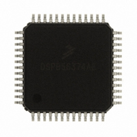
Manufacturer Part Number
DSPB56374AE
Description
IC DSP 24BIT 150MHZ 52-LQFP
Manufacturer
Freescale Semiconductor
Series
Symphony™r
Type
Audio Processorr
Datasheet
1.DSPB56374AE.pdf
(64 pages)
Specifications of DSPB56374AE
Interface
Host Interface, I²C, SAI, SPI
Clock Rate
150MHz
Non-volatile Memory
ROM (84 kB)
On-chip Ram
54kB
Voltage - I/o
3.30V
Voltage - Core
1.25V
Operating Temperature
-40°C ~ 110°C
Mounting Type
Surface Mount
Package / Case
52-LQFP
Product
DSPs
Data Bus Width
24 bit
Processor Series
DSP563xx
Core
56000
Numeric And Arithmetic Format
Fixed-Point
Device Million Instructions Per Second
150 MIPS
Maximum Clock Frequency
150 MHz
Program Memory Type
Flash
Program Memory Size
24 KB
Data Ram Size
54 KB
Operating Supply Voltage
1.25 V or 3.3 V
Maximum Operating Temperature
+ 110 C
Mounting Style
SMD/SMT
Interface Type
SIA, SHI
Minimum Operating Temperature
- 40 C
Leaded Process Compatible
Yes
Rohs Compliant
Yes
Peak Reflow Compatible (260 C)
Yes
Lead Free Status / Rohs Status
Lead free / RoHS Compliant
Available stocks
Company
Part Number
Manufacturer
Quantity
Price
Company:

Part Number:
DSPB56374AE
Manufacturer:
DELPHI
Quantity:
10 000
Company:
Part Number:
DSPB56374AE
Manufacturer:
QFP
Quantity:
591
Company:
Part Number:
DSPB56374AE
Manufacturer:
Freescale Semiconductor
Quantity:
10 000
Part Number:
DSPB56374AE
Manufacturer:
FREESCALE
Quantity:
20 000
Company:
Part Number:
DSPB56374AEC
Manufacturer:
Freescale Semiconductor
Quantity:
10 000


Signal Groupings
4.1
4.2
6
CORE_VDD (4)
PLLA_VDD (1)
PLLD_VDD (1)
Dedicated GPIO
Timer
JTAG/OnCE Port
Note:
PLLP_VDD(1)
Power Name
Ground Name
PLLA_GND(1)
(80-pin 4)
(52-pin 3)
1
2
3
4
5
IO_VDD
Power
Ground
Pins are not 5 V. tolerant unless noted.
Port H signals are the GPIO port signals which are multiplexed with the MOD and HREQ signals.
Port G signals are the dedicated GPIO port signals.
Port C signals are the GPIO port signals which are multiplexed with the ESAI signals.
Port E signals are the GPIO port signals which are multiplexed with the ESAI_1 signals.
PLL Power— The voltage (3.3 V) should be well-regulated and the input should be provided with
an extremely low impedance path to the 3.3 V
external decoupling capacitors between PLLA_VDD and PLLA_GND. PLLA_VDD requires a filter
as shown in Figure 1 and Figure 2 below. See the DSP56374 technical data sheet for additional
details.
PLL Power— The voltage (3.3 V) should be well-regulated and the input should be provided with
an extremely low impedance path to the 3.3 V
external decoupling capacitors between PLLP_VDD and PLLP_GND.
PLL Power— The voltage (1.25 V) should be well-regulated and the input should be provided with
an extremely low impedance path to the 1.25 V
external decoupling capacitors between PLLD_VDD and PLLD_GND.
Core Power—The voltage (1.25 V) should be well-regulated and the input should be provided with
an extremely low impedance path to the 1.25 V
external decoupling capacitors.
SHI, ESAI, ESAI_1, WDT and Timer I/O Power —The voltage (3.3 V) should be well-regulated,
and the input should be provided with an extremely low impedance path to the 3.3 V
This is an isolated power for the SHI, ESAI, ESAI_1, WDT and Timer I/O. The user must provide
adequate external decoupling capacitors.
PLL Ground—The PLL ground should be provided with an extremely low-impedance path to
ground. This connection must be tied externally to all other chip ground connections. The user
must provide adequate external decoupling capacitors between PLLA_VDD and PLLA_GND.
Table 3. DSP56374 Functional Signal Groupings (continued)
Functional Group
DSP56374 Data Sheet, Rev. 4.2
Table 4. Power Inputs
Table 5. Grounds
Description
Description
Port G
DD
DD
DD
DD
power rail. The user must provide adequate
power rail. The user must provide adequate
3
power rail. The user must provide adequate
power rail. The user must provide adequate
Number of
Signals
15
3
4
1
Freescale Semiconductor
Description
Detailed
Table 12
Table 13
Table 14
DD
power rail.
Related parts for DSPB56374AE
Image
Part Number
Description
Manufacturer
Datasheet
Request
R

Part Number:
Description:
Manufacturer:
Freescale Semiconductor, Inc
Datasheet:
Part Number:
Description:
Manufacturer:
Freescale Semiconductor, Inc
Datasheet:
Part Number:
Description:
Manufacturer:
Freescale Semiconductor, Inc
Datasheet:
Part Number:
Description:
Manufacturer:
Freescale Semiconductor, Inc
Datasheet:
Part Number:
Description:
Manufacturer:
Freescale Semiconductor, Inc
Datasheet:
Part Number:
Description:
Manufacturer:
Freescale Semiconductor, Inc
Datasheet:
Part Number:
Description:
Manufacturer:
Freescale Semiconductor, Inc
Datasheet:
Part Number:
Description:
Manufacturer:
Freescale Semiconductor, Inc
Datasheet:
Part Number:
Description:
Manufacturer:
Freescale Semiconductor, Inc
Datasheet:
Part Number:
Description:
Manufacturer:
Freescale Semiconductor, Inc
Datasheet:
Part Number:
Description:
Manufacturer:
Freescale Semiconductor, Inc
Datasheet:
Part Number:
Description:
Manufacturer:
Freescale Semiconductor, Inc
Datasheet:
Part Number:
Description:
Manufacturer:
Freescale Semiconductor, Inc
Datasheet:
Part Number:
Description:
Manufacturer:
Freescale Semiconductor, Inc
Datasheet:
Part Number:
Description:
Manufacturer:
Freescale Semiconductor, Inc
Datasheet: