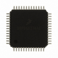
DSPB56374AE Freescale Semiconductor, DSPB56374AE Datasheet - Page 51

DSPB56374AE
Manufacturer Part Number
DSPB56374AE
Description
IC DSP 24BIT 150MHZ 52-LQFP
Manufacturer
Freescale Semiconductor
Series
Symphony™r
Type
Audio Processorr
Datasheet
1.DSPB56374AE.pdf
(64 pages)
Specifications of DSPB56374AE
Interface
Host Interface, I²C, SAI, SPI
Clock Rate
150MHz
Non-volatile Memory
ROM (84 kB)
On-chip Ram
54kB
Voltage - I/o
3.30V
Voltage - Core
1.25V
Operating Temperature
-40°C ~ 110°C
Mounting Type
Surface Mount
Package / Case
52-LQFP
Product
DSPs
Data Bus Width
24 bit
Processor Series
DSP563xx
Core
56000
Numeric And Arithmetic Format
Fixed-Point
Device Million Instructions Per Second
150 MIPS
Maximum Clock Frequency
150 MHz
Program Memory Type
Flash
Program Memory Size
24 KB
Data Ram Size
54 KB
Operating Supply Voltage
1.25 V or 3.3 V
Maximum Operating Temperature
+ 110 C
Mounting Style
SMD/SMT
Interface Type
SIA, SHI
Minimum Operating Temperature
- 40 C
Leaded Process Compatible
Yes
Rohs Compliant
Yes
Peak Reflow Compatible (260 C)
Yes
Lead Free Status / Rohs Status
Lead free / RoHS Compliant
Available stocks
Company
Part Number
Manufacturer
Quantity
Price
Company:
Part Number:
DSPB56374AE
Manufacturer:
DELPHI
Quantity:
10 000
Company:
Part Number:
DSPB56374AE
Manufacturer:
QFP
Quantity:
591
Company:
Part Number:
DSPB56374AE
Manufacturer:
Freescale Semiconductor
Quantity:
10 000
Part Number:
DSPB56374AE
Manufacturer:
FREESCALE
Quantity:
20 000
Company:
Part Number:
DSPB56374AEC
Manufacturer:
Freescale Semiconductor
Quantity:
10 000
Freescale Semiconductor
Note:
No.
109
110
111
112
113
114
115
116
117
118
119
(Input)
1. V
2. All timings apply to OnCE module data transfers because it uses the JTAG port as an interface.
TCK cycle time in Crystal mode
TCK clock pulse width measured at 1.65 V
TCK rise and fall times
Boundary scan input data setup time
Boundary scan input data hold time
TCK low to output data valid
TCK low to output high impedance
TMS, TDI data setup time
TMS, TDI data hold time
TCK low to TDO data valid
TCK low to TDO high impedance
TCK
CORE_VDD
= 1.25 V ± 0.05 V; T
111
Figure 18. Test Clock Input Timing Diagram
Characteristics
V
IH
Table 27. JTAG Timing (continued)
J
DSP56374 Data Sheet, Rev. 4.2
= -40°C to 110°C (52 LQFP) / -40°C to 105°C (80 LQFP), C
V
IL
V
110
M
109
111
100.0
50.0
15.0
24.0
25.0
Min
5.0
110
V
All frequencies
—
—
—
—
—
M
Max
40.0
40.0
44.0
44.0
3.0
—
—
—
—
—
—
L
= 50 pF
Unit
ns
ns
ns
ns
ns
ns
ns
ns
ns
ns
ns
JTAG Timing
51


