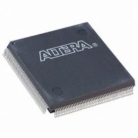
EP2C5Q208C7N Altera, EP2C5Q208C7N Datasheet - Page 158

EP2C5Q208C7N
Manufacturer Part Number
EP2C5Q208C7N
Description
IC CYCLONE II FPGA 5K 208-PQFP
Manufacturer
Altera
Series
Cyclone® IIr
Datasheet
1.EP2C5T144C8N.pdf
(168 pages)
Specifications of EP2C5Q208C7N
Number Of Logic Elements/cells
4608
Number Of Labs/clbs
288
Total Ram Bits
119808
Number Of I /o
142
Voltage - Supply
1.15 V ~ 1.25 V
Mounting Type
Surface Mount
Operating Temperature
0°C ~ 85°C
Package / Case
208-MQFP, 208-PQFP
Family Name
Cyclone® II
Number Of Logic Blocks/elements
4608
# I/os (max)
142
Frequency (max)
402.58MHz
Process Technology
90nm
Operating Supply Voltage (typ)
1.2V
Logic Cells
4608
Ram Bits
119808
Operating Supply Voltage (min)
1.15V
Operating Supply Voltage (max)
1.25V
Operating Temp Range
0C to 85C
Operating Temperature Classification
Commercial
Mounting
Surface Mount
Pin Count
208
Package Type
PQFP
Lead Free Status / RoHS Status
Lead free / RoHS Compliant
Number Of Gates
-
Lead Free Status / Rohs Status
Compliant
Other names
544-1674
Available stocks
Company
Part Number
Manufacturer
Quantity
Price
Company:
Part Number:
EP2C5Q208C7N
Manufacturer:
ALTERA
Quantity:
45
Part Number:
EP2C5Q208C7N
Manufacturer:
ALTERA/阿尔特拉
Quantity:
20 000
Duty Cycle Distortion
Figure 5–9. DCD Measurement Technique for Non-DDIO (Single-Data Rate) Outputs
5–68
Cyclone II Device Handbook, Volume 1
clk
DCD Measurement Techniques
DCD is measured at an FPGA output pin driven by registers inside the
corresponding I/O element (IOE) block. When the output is a single data
rate signal (non-DDIO), only one edge of the register input clock (positive
or negative) triggers output transitions
present on the input clock signal, or caused by the clock input buffer, or
different input I/O standard, does not transfer to the output signal.
However, when the output is a double data rate input/output (DDIO)
signal, both edges of the input clock signal (positive and negative) trigger
output transitions
clock and the input clock buffer affect the output DCD.
IOE
(T/2 – D1) / T (the low percentage boundary)
(T/2 + D2) / T (the high percentage boundary)
(Figure
DFF
D
5–10). Therefore, any distortion on the input
Q
(Figure
5–9). Therefore, any DCD
Altera Corporation
output
February 2008


