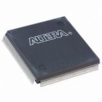
EP2C5Q208C7N Altera, EP2C5Q208C7N Datasheet - Page 80

EP2C5Q208C7N
Manufacturer Part Number
EP2C5Q208C7N
Description
IC CYCLONE II FPGA 5K 208-PQFP
Manufacturer
Altera
Series
Cyclone® IIr
Datasheet
1.EP2C5T144C8N.pdf
(168 pages)
Specifications of EP2C5Q208C7N
Number Of Logic Elements/cells
4608
Number Of Labs/clbs
288
Total Ram Bits
119808
Number Of I /o
142
Voltage - Supply
1.15 V ~ 1.25 V
Mounting Type
Surface Mount
Operating Temperature
0°C ~ 85°C
Package / Case
208-MQFP, 208-PQFP
Family Name
Cyclone® II
Number Of Logic Blocks/elements
4608
# I/os (max)
142
Frequency (max)
402.58MHz
Process Technology
90nm
Operating Supply Voltage (typ)
1.2V
Logic Cells
4608
Ram Bits
119808
Operating Supply Voltage (min)
1.15V
Operating Supply Voltage (max)
1.25V
Operating Temp Range
0C to 85C
Operating Temperature Classification
Commercial
Mounting
Surface Mount
Pin Count
208
Package Type
PQFP
Lead Free Status / RoHS Status
Lead free / RoHS Compliant
Number Of Gates
-
Lead Free Status / Rohs Status
Compliant
Other names
544-1674
Available stocks
Company
Part Number
Manufacturer
Quantity
Price
Company:
Part Number:
EP2C5Q208C7N
Manufacturer:
ALTERA
Quantity:
45
Part Number:
EP2C5Q208C7N
Manufacturer:
ALTERA/阿尔特拉
Quantity:
20 000
Configuration Schemes
Configuration
Schemes
3–6
Cyclone II Device Handbook, Volume 1
Active serial (AS)
Passive serial (PS) Enhanced or EPC2 configuration device, MasterBlaster, ByteBlasterMV, ByteBlaster II or
JTAG
Table 3–4. Data Sources for Configuration
Configuration
Scheme
f
Low-cost serial configuration device
USB Blaster download cable, or serial data source
microprocessor with a Jam or JBC file
MasterBlaster, ByteBlasterMV, ByteBlaster II or USB Blaster download cable or a
SRAM configuration elements allow Cyclone II devices to be
reconfigured in-circuit by loading new configuration data into the device.
With real-time reconfiguration, the device is forced into command mode
with the nCONFIG pin. The configuration process loads different
configuration data, reinitializes the device, and resumes user-mode
operation. You can perform in-field upgrades by distributing new
configuration files within the system or remotely.
A built-in weak pull-up resistor pulls all user I/O pins to V
and during device configuration.
The configuration pins support 1.5-V/1.8-V or 2.5-V/3.3-V I/O
standards. The voltage level of the configuration output pins is
determined by the V
V
3.3-V compatible.
You can load the configuration data for a Cyclone II device with one of
three configuration schemes (see
target application. You can use a configuration device, intelligent
controller, or the JTAG port to configure a Cyclone II device. A low-cost
configuration device can automatically configure a Cyclone II device at
system power-up.
Multiple Cyclone II devices can be configured in any of the three
configuration schemes by connecting the configuration enable (nCE) and
configuration enable output (nCEO) pins on each device.
For more information on configuration, see the Configuring Cyclone II
Devices chapter of the Cyclone II Handbook, Volume 2.
CCIO
selects whether the configuration inputs are 1.5-V, 1.8-V, 2.5-V, or
CCIO
of the bank where the pins reside. The bank
Data Source
Table
3–4), chosen on the basis of the
Altera Corporation
February 2007
CCIO
before


