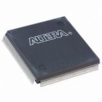
EP2C5Q208C7N Altera, EP2C5Q208C7N Datasheet - Page 59

EP2C5Q208C7N
Manufacturer Part Number
EP2C5Q208C7N
Description
IC CYCLONE II FPGA 5K 208-PQFP
Manufacturer
Altera
Series
Cyclone® IIr
Datasheet
1.EP2C5T144C8N.pdf
(168 pages)
Specifications of EP2C5Q208C7N
Number Of Logic Elements/cells
4608
Number Of Labs/clbs
288
Total Ram Bits
119808
Number Of I /o
142
Voltage - Supply
1.15 V ~ 1.25 V
Mounting Type
Surface Mount
Operating Temperature
0°C ~ 85°C
Package / Case
208-MQFP, 208-PQFP
Family Name
Cyclone® II
Number Of Logic Blocks/elements
4608
# I/os (max)
142
Frequency (max)
402.58MHz
Process Technology
90nm
Operating Supply Voltage (typ)
1.2V
Logic Cells
4608
Ram Bits
119808
Operating Supply Voltage (min)
1.15V
Operating Supply Voltage (max)
1.25V
Operating Temp Range
0C to 85C
Operating Temperature Classification
Commercial
Mounting
Surface Mount
Pin Count
208
Package Type
PQFP
Lead Free Status / RoHS Status
Lead free / RoHS Compliant
Number Of Gates
-
Lead Free Status / Rohs Status
Compliant
Other names
544-1674
Available stocks
Company
Part Number
Manufacturer
Quantity
Price
Company:
Part Number:
EP2C5Q208C7N
Manufacturer:
ALTERA
Quantity:
45
Part Number:
EP2C5Q208C7N
Manufacturer:
ALTERA/阿尔特拉
Quantity:
20 000
Altera Corporation
February 2007
Notes to
(1)
(2)
(3)
(4)
(5)
(6)
EP2C35
EP2C50
EP2C70
Table 2–15. Cyclone II DQS & DQ Bus Mode Support (Part 2 of 2)
Device
Numbers are preliminary.
EP2C5 and EP2C8 devices in the 144-pin TQFP package do not have any DQ pin groups in I/O bank 1.
Because of available clock resources, only a total of 6 DQ/DQS groups can be implemented.
Because of available clock resources, only a total of 14 DQ/DQS groups can be implemented.
The ×9 DQS/DQ groups are also used as ×8 DQS/DQ groups. The ×18 DQS/DQ groups are also used as ×16
DQS/DQ groups.
For QDRI implementation, if you connect the D ports (write data) to the Cyclone II DQ pins, the total available ×9
DQS /DQ and ×18 DQS/DQ groups are half of that shown in
Table
2–15:
484-pin FineLine BGA
672-pin FineLine BGA
484-pin FineLine BGA
672-pin FineLine BGA
672-pin FineLine BGA
896-pin FineLine BGA
Package
You can use any of the DQ pins for the parity pins in Cyclone II devices.
The Cyclone II device family supports parity in the ×8/×9, and ×16/×18
mode. There is one parity bit available per eight bits of data pins.
The data mask, DM, pins are required when writing to DDR SDRAM and
DDR2 SDRAM devices. A low signal on the DM pin indicates that the
write is valid. If the DM signal is high, the memory masks the DQ signals.
In Cyclone II devices, the DM pins are assigned and are the preferred
pins. Each group of DQS and DQ signals requires a DM pin.
When using the Cyclone II I/O banks to interface with the DDR memory,
at least one PLL with two clock outputs is needed to generate the system
and write clock. The system clock is used to clock the DQS write signals,
commands, and addresses. The write clock is shifted by –90° from the
system clock and is used to clock the DQ signals during writes.
Figure 2–27
the dedicated circuitry to the logic array.
Number of ×8
illustrates DDR SDRAM interfacing from the I/O through
Groups
16
20
16
20
20
20
(4)
(4)
(4)
(4)
(4)
(4)
Groups (5),
Number of ×9
Table
8
8
8
8
8
8
2–15.
Cyclone II Device Handbook, Volume 1
(6)
Note (1)
Number of ×16
Groups
8
8
8
8
8
8
Cyclone II Architecture
Number of ×18
Groups (5),
8
8
8
8
8
8
2–47
(6)


