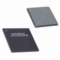
EP1C4F400C8N Altera, EP1C4F400C8N Datasheet - Page 43

EP1C4F400C8N
Manufacturer Part Number
EP1C4F400C8N
Description
IC CYCLONE FPGA 4K LE 400-FBGA
Manufacturer
Altera
Series
Cyclone®r
Datasheet
1.EP1C3T144C8.pdf
(106 pages)
Specifications of EP1C4F400C8N
Number Of Logic Elements/cells
4000
Number Of Labs/clbs
400
Total Ram Bits
78336
Number Of I /o
301
Voltage - Supply
1.425 V ~ 1.575 V
Mounting Type
Surface Mount
Operating Temperature
0°C ~ 85°C
Package / Case
400-FBGA
Lead Free Status / RoHS Status
Lead free / RoHS Compliant
Number Of Gates
-
Other names
544-1806
EP1C4F400C8N
EP1C4F400C8N
Available stocks
Company
Part Number
Manufacturer
Quantity
Price
Company:
Part Number:
EP1C4F400C8N
Manufacturer:
CYCLONE
Quantity:
5 510
Company:
Part Number:
EP1C4F400C8N
Manufacturer:
ALTERA
Quantity:
104
Part Number:
EP1C4F400C8N
Manufacturer:
ALTERA/阿尔特拉
Quantity:
20 000
Company:
Part Number:
EP1C4F400C8NAA
Manufacturer:
ALTERA
Quantity:
3 000
Company:
Part Number:
EP1C4F400C8NAB
Manufacturer:
ALTERA
Quantity:
3 000
Altera Corporation
May 2008
does not have dedicated clock output pins. The EP1C6 device in the
144-pin TQFP package only supports dedicated clock outputs from
PLL 1.
Clock Feedback
Cyclone PLLs have three modes for multiplication and/or phase shifting:
■
■
■
Phase Shifting
Cyclone PLLs have an advanced clock shift capability that enables
programmable phase shifts. You can enter a phase shift (in degrees or
time units) for each PLL clock output port or for all outputs together in
one shift. You can perform phase shifting in time units with a resolution
range of 125 to 250 ps. The finest resolution equals one eighth of the VCO
period. The VCO period is a function of the frequency input and the
multiplication and division factors. Each clock output counter can choose
a different phase of the VCO period from up to eight taps. You can use this
clock output counter along with an initial setting on the post-scale
counter to achieve a phase-shift range for the entire period of the output
clock. The phase tap feedback to the m counter can shift all outputs to a
single phase. The Quartus II software automatically sets the phase taps
and counter settings according to the phase shift entered.
Lock Detect Signal
The lock output indicates that there is a stable clock output signal in
phase with the reference clock. Without any additional circuitry, the lock
signal may toggle as the PLL begins tracking the reference clock.
Therefore, you may need to gate the lock signal for use as a
system-control signal. For correct operation of the lock circuit below
–20 C, f
Zero delay buffer mode⎯ The external clock output pin is phase-
aligned with the clock input pin for zero delay.
Normal mode⎯ If the design uses an internal PLL clock output, the
normal mode compensates for the internal clock delay from the input
clock pin to the IOE registers. The external clock output pin is phase
shifted with respect to the clock input pin if connected in this mode.
You defines which internal clock output from the PLL should be
phase-aligned to compensate for internal clock delay.
No compensation mode⎯ In this mode, the PLL will not compensate
for any clock networks.
IN/N
> 200 MHz.
Global Clock Network and Phase-Locked Loops
Preliminary
2–37


