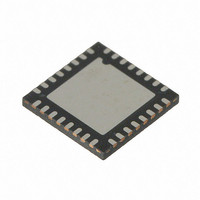
CY8CTST200-32LQXI Cypress Semiconductor Corp, CY8CTST200-32LQXI Datasheet - Page 100

CY8CTST200-32LQXI
Manufacturer Part Number
CY8CTST200-32LQXI
Description
IC MCU 32K FLASH 32UQFN
Manufacturer
Cypress Semiconductor Corp
Series
TrueTouch™r
Datasheet
1.CY8CTST200-16LGXI.pdf
(308 pages)
Specifications of CY8CTST200-32LQXI
Program Memory Type
FLASH (32 kB)
Package / Case
32-UQFN Exposed Pad, 32-HUQFN, 32-SQFN
Applications
Touchscreen Controller
Core Processor
M8C
Controller Series
CY8CT
Ram Size
2K x 8
Interface
I²C, SPI, UART/USART, USB
Number Of I /o
28
Voltage - Supply
1.8 V
Operating Temperature
-40°C ~ 85°C
Mounting Type
Surface Mount
Processor Series
CY8CTxx2xx
Core
M8C
Data Bus Width
8 bit
Data Ram Size
2 KB
Interface Type
I2C, SPI
Maximum Clock Frequency
24 MHz
Number Of Timers
3
Operating Supply Voltage
1.71 V to 5.5 V
Mounting Style
SMD/SMT
Program Memory Size
32 KB
Lead Free Status / RoHS Status
Lead free / RoHS Compliant
For Use With
770-1000 - ISP 4PORT FOR CYPRESS PSOC MCU
Lead Free Status / Rohs Status
Lead free / RoHS Compliant
Other names
428-2957
- Current page: 100 of 308
- Download datasheet (3Mb)
12.2
The following registers are only associated with the Analog Bus Mux in the CY8CTMG20x and CY8CTST200 PSoC devices
and are listed in address order. Each register description has an associated register table showing the bit structure for that
register. Register bits that are grayed out throughout this document are reserved bits and are not detailed in the register
descriptions that follow. Always write reserved bits with a value of ‘0’.
12.2.1
The Analog Mux Port Bit Enable Registers (MUX_CR0,
MUX_CR1, MUX_CR2, MUX_CR3, and MUX_CR4) control
the connection between the analog mux bus and the corre-
sponding pin.
Bits 7 to 0: ENABLE[7:0]. The bits in these registers
enable connection of individual pins to the analog mux bus.
Each I/O port has a corresponding MUX_CRx register.
I/O Analog Multiplexer
100
1,D8h
1,D9h
1,DAh
1,DBh
1,DFh
Address
MUX_CR0
MUX_CR1
MUX_CR2
MUX_CR3
MUX_CR4
Register Definitions
MUX_CRx Registers
Name
Bit 7
Bit 6
PSoC CY8CTMG20x and CY8CTST200 TRM, Document No. 001-53603 Rev. *C
Bit 5
Bit 4
ENABLE[7:0]
ENABLE[7:0]
ENABLE[7:0]
ENABLE[7:0]
Setting a bit high connects the corresponding pin to the
analog bus.
For additional information, refer to the
page
271.
Bit 3
Bit 2
ENABLE[3:0]
Bit 1
MUX_CRx register on
Bit 0
RW : 00
RW : 00
RW : 00
RW : 00
Access
RW : 0
[+] Feedback
Related parts for CY8CTST200-32LQXI
Image
Part Number
Description
Manufacturer
Datasheet
Request
R
Part Number:
Description:
CY8CTST200-24LQXIT
Manufacturer:
Cypress Semiconductor Corp
Datasheet:
Part Number:
Description:
CY8CTST200-32LQXIT
Manufacturer:
Cypress Semiconductor Corp
Datasheet:
Part Number:
Description:
IC MCU 32K FLASH 16-QFN
Manufacturer:
Cypress Semiconductor Corp
Datasheet:
Part Number:
Description:
IC MCU 32K FLASH 24UQFN
Manufacturer:
Cypress Semiconductor Corp
Datasheet:
Part Number:
Description:
IC MCU 32K FLASH 48-QFN
Manufacturer:
Cypress Semiconductor Corp
Datasheet:
Part Number:
Description:
IC MCU 32K FLASH 48-SSOP
Manufacturer:
Cypress Semiconductor Corp
Datasheet:
Part Number:
Description:
IC MCU 32K FLASH 48-QFN
Manufacturer:
Cypress Semiconductor Corp
Datasheet:
Part Number:
Description:
IC MCU 32K FLASH 16-QFN
Manufacturer:
Cypress Semiconductor Corp
Part Number:
Description:
IC MCU 32K FLASH 48-SSOP
Manufacturer:
Cypress Semiconductor Corp
Part Number:
Description:
Manufacturer:
Cypress Semiconductor Corp
Datasheet:


