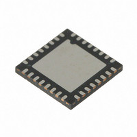
CY8CTST200-32LQXI Cypress Semiconductor Corp, CY8CTST200-32LQXI Datasheet - Page 220

CY8CTST200-32LQXI
Manufacturer Part Number
CY8CTST200-32LQXI
Description
IC MCU 32K FLASH 32UQFN
Manufacturer
Cypress Semiconductor Corp
Series
TrueTouch™r
Datasheet
1.CY8CTST200-16LGXI.pdf
(308 pages)
Specifications of CY8CTST200-32LQXI
Program Memory Type
FLASH (32 kB)
Package / Case
32-UQFN Exposed Pad, 32-HUQFN, 32-SQFN
Applications
Touchscreen Controller
Core Processor
M8C
Controller Series
CY8CT
Ram Size
2K x 8
Interface
I²C, SPI, UART/USART, USB
Number Of I /o
28
Voltage - Supply
1.8 V
Operating Temperature
-40°C ~ 85°C
Mounting Type
Surface Mount
Processor Series
CY8CTxx2xx
Core
M8C
Data Bus Width
8 bit
Data Ram Size
2 KB
Interface Type
I2C, SPI
Maximum Clock Frequency
24 MHz
Number Of Timers
3
Operating Supply Voltage
1.71 V to 5.5 V
Mounting Style
SMD/SMT
Program Memory Size
32 KB
Lead Free Status / RoHS Status
Lead free / RoHS Compliant
For Use With
770-1000 - ISP 4PORT FOR CYPRESS PSOC MCU
Lead Free Status / Rohs Status
Lead free / RoHS Compliant
Other names
428-2957
- Current page: 220 of 308
- Download datasheet (3Mb)
PRS_CR
21.3.32 PRS_CR
This register controls the Prescaler and Pseudo Random Sequence generator output. For additional information, refer to the
Register Definitions on page 92
Bit
7
6
5
4
3
2:0
220
Individual Register Names and Addresses:
PRS_CR : 0,A9h
Access : POR
Bit Name
0,A9h
CS_CLK_OUT
CS_CLK_INV
PRS_12BIT
PRS_EN
PRESCALEBYP
PRESCALE_CLK_DIV[2:0] These bits allow for of one of eight frequencies of incoming IMO clock to be fed as input to PRS.
Name
CS_CLK_OUT
Pseudo Ransom Sequence and Prescaler Control Register
RW : 0
7
CS_CLK_INV
RW : 0‘
in the TrueTouch Module chapter .
6
Description
This bit selects the TrueTouch clock (inversion or non-inversion depending on bit 6 setting) to be
routed onto primary pin depending on the OUT_P1/OUT_P0 register selection.
1
0
This bit allows you to route either TrueTouch clock or inversion of the TrueTouch clock onto pin.
1
0
This bit allows selection between 8-bit PRS or 12-bit PRS output.
0
1
This bit is used to enable or disable the PRS block.
0
1
This bit is used to bypass the prescaler and pass the input clock undivided onto the output. The out-
put of the prescaler feeds the clock input to the PRS block.
0
1
000
001
010
011
100
101
110
111
PSoC CY8CTMG20x and CY8CTST200 TRM, Document No. 001-53603 Rev. *C
PRS_12BIT
Route prescaler output or PRS output depending on CSD_PRSCLK in CS_CR0 when in
CSD mode, or route clock based on CLKSEL bits in CS_CR1 register in normal TrueTouch
mode to primary pins P1[2]/P0[7] depending on OUT_P1/OUT_P0 bit selections instead of
normal CSOUT[ selections. See OUT_P1/OUT_P0 registers for details.
Use CSOUT [1:0] selections as normal.
Inverted TrueTouch clock routes to pin (see bit 7).
Non-inverted TrueTouch clock routes to pin (see bit 7).
MSB of 8-bit PRS is sent out.
MSB of 12-bit PRS is sent out
PRS is disabled. PRS block output is '0'.
PRS is enabled and the bit 5 decides whether MSB of 12-bit PRS is sent out or MSB of 8-bit
PRS is sent out.
Divided clock is sent out of prescaler depending on bit [2:0] setting.
Incoming IMO clock is sent out of prescaler without any division.
Divides the input IMO clock by 2.
Divides the input IMO clock by 4.
Divides the input IMO clock by 8.
Divides the input IMO clock by 16.
Divides the input IMO clock by 32.
Divides the input IMO clock by 64.
Divides the input IMO clock by 128.
Divides the input IMO clock by 256.
RW : 0‘
5
PRS_EN
RW : 0
4
PRESCALE-
RW : 0
BYP
3
2
PRESCALE_CLK_DIV[2:0]
RW : 0
1
0,A9h
0
[+] Feedback
Related parts for CY8CTST200-32LQXI
Image
Part Number
Description
Manufacturer
Datasheet
Request
R
Part Number:
Description:
CY8CTST200-24LQXIT
Manufacturer:
Cypress Semiconductor Corp
Datasheet:
Part Number:
Description:
CY8CTST200-32LQXIT
Manufacturer:
Cypress Semiconductor Corp
Datasheet:
Part Number:
Description:
IC MCU 32K FLASH 16-QFN
Manufacturer:
Cypress Semiconductor Corp
Datasheet:
Part Number:
Description:
IC MCU 32K FLASH 24UQFN
Manufacturer:
Cypress Semiconductor Corp
Datasheet:
Part Number:
Description:
IC MCU 32K FLASH 48-QFN
Manufacturer:
Cypress Semiconductor Corp
Datasheet:
Part Number:
Description:
IC MCU 32K FLASH 48-SSOP
Manufacturer:
Cypress Semiconductor Corp
Datasheet:
Part Number:
Description:
IC MCU 32K FLASH 48-QFN
Manufacturer:
Cypress Semiconductor Corp
Datasheet:
Part Number:
Description:
IC MCU 32K FLASH 16-QFN
Manufacturer:
Cypress Semiconductor Corp
Part Number:
Description:
IC MCU 32K FLASH 48-SSOP
Manufacturer:
Cypress Semiconductor Corp
Part Number:
Description:
Manufacturer:
Cypress Semiconductor Corp
Datasheet:


