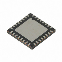
CY8CTST200-32LQXI Cypress Semiconductor Corp, CY8CTST200-32LQXI Datasheet - Page 63

CY8CTST200-32LQXI
Manufacturer Part Number
CY8CTST200-32LQXI
Description
IC MCU 32K FLASH 32UQFN
Manufacturer
Cypress Semiconductor Corp
Series
TrueTouch™r
Datasheet
1.CY8CTST200-16LGXI.pdf
(308 pages)
Specifications of CY8CTST200-32LQXI
Program Memory Type
FLASH (32 kB)
Package / Case
32-UQFN Exposed Pad, 32-HUQFN, 32-SQFN
Applications
Touchscreen Controller
Core Processor
M8C
Controller Series
CY8CT
Ram Size
2K x 8
Interface
I²C, SPI, UART/USART, USB
Number Of I /o
28
Voltage - Supply
1.8 V
Operating Temperature
-40°C ~ 85°C
Mounting Type
Surface Mount
Processor Series
CY8CTxx2xx
Core
M8C
Data Bus Width
8 bit
Data Ram Size
2 KB
Interface Type
I2C, SPI
Maximum Clock Frequency
24 MHz
Number Of Timers
3
Operating Supply Voltage
1.71 V to 5.5 V
Mounting Style
SMD/SMT
Program Memory Size
32 KB
Lead Free Status / RoHS Status
Lead free / RoHS Compliant
For Use With
770-1000 - ISP 4PORT FOR CYPRESS PSOC MCU
Lead Free Status / Rohs Status
Lead free / RoHS Compliant
Other names
428-2957
- Current page: 63 of 308
- Download datasheet (3Mb)
This chapter presents the Internal Main Oscillator (IMO) and its associated registers. The IMO produces clock signals of 6,
12, and 24 MHz. For a complete table of the IMO registers, refer to the
a quick reference of allPSoC registers in address order, refer to the
7.1
The Internal Main Oscillator (IMO) outputs a clock that is
normally driven to the main system clock, SYSCLK. The
IMO clock frequency can be configured as 6, 12, or 24 MHz.
The accuracy of the internal IMO clock is approximately
±5% over temperature and voltage variation. No external
components are required to achieve this level of accuracy.
The IMO provides higher accuracies when enabled for lock-
ing to USB traffic during USB operation. See
USB chapter on page 165
can be disabled when using an external clocking source.
Also, the frequency doubler circuit, which produces
SYSCLKX2, can be disabled to save power. When using an
external clock, and SYSCLKX2 is needed, you cannot dis-
able the IMO.
Registers for controlling these operations are found in the
Digital Clocks chapter on page
Table 7-1. IMO Frequencies
PSoC CY8CTMG20x and CY8CTST200 TRM, Document No. 001-53603 Rev. *C
00
01
10
11
7. Internal Main Oscillator (IMO)
SLIMO
Architectural Description
12
6
24
Reserved
CY8CTMG20x, CY8CTST200
for more information. The IMO
109.
Full-Speed
7.2
Device power may be optimized by selecting among the 24,
12, or 6 MHz settings using the SLIMO bits in the
CPU_SCR1 register in conjunction with associated trim val-
ues in the IMO_TR register. Both methods are described
ahead.
7.2.1
An 8-bit register (IMO_TR) is used to trim the IMO. Bit 0 is
the LSB and bit 7 is the MSB. The trim step size is approxi-
mately 60 kHz at the 24 MHz clock setting. A factory trim
setting is loaded into the IMO_TR register at boot time.
7.2.2
Writing to the SLIMO bits of the CPU_SCR1 register
enables the Slow IMO feature. SLIMO settings for 6 and 12
MHz are listed in
ranges, the associated factory trim value must be loaded
into the IMO_TR register. The IMO immediately changes to
the new frequency. Factory trim settings are stored in Flash
for the frequencies listed in
Register Reference chapter on page
Summary Table of the Core Registers on page
Application Overview
Trimming the IMO
Engaging Slow IMO
Table
7-1. When changing frequency
Table
7-1.
187.
24. For
[+] Feedback
63
Related parts for CY8CTST200-32LQXI
Image
Part Number
Description
Manufacturer
Datasheet
Request
R
Part Number:
Description:
CY8CTST200-24LQXIT
Manufacturer:
Cypress Semiconductor Corp
Datasheet:
Part Number:
Description:
CY8CTST200-32LQXIT
Manufacturer:
Cypress Semiconductor Corp
Datasheet:
Part Number:
Description:
IC MCU 32K FLASH 16-QFN
Manufacturer:
Cypress Semiconductor Corp
Datasheet:
Part Number:
Description:
IC MCU 32K FLASH 24UQFN
Manufacturer:
Cypress Semiconductor Corp
Datasheet:
Part Number:
Description:
IC MCU 32K FLASH 48-QFN
Manufacturer:
Cypress Semiconductor Corp
Datasheet:
Part Number:
Description:
IC MCU 32K FLASH 48-SSOP
Manufacturer:
Cypress Semiconductor Corp
Datasheet:
Part Number:
Description:
IC MCU 32K FLASH 48-QFN
Manufacturer:
Cypress Semiconductor Corp
Datasheet:
Part Number:
Description:
IC MCU 32K FLASH 16-QFN
Manufacturer:
Cypress Semiconductor Corp
Part Number:
Description:
IC MCU 32K FLASH 48-SSOP
Manufacturer:
Cypress Semiconductor Corp
Part Number:
Description:
Manufacturer:
Cypress Semiconductor Corp
Datasheet:


