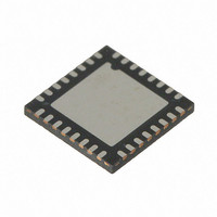
CY8CTST200-32LQXI Cypress Semiconductor Corp, CY8CTST200-32LQXI Datasheet - Page 260

CY8CTST200-32LQXI
Manufacturer Part Number
CY8CTST200-32LQXI
Description
IC MCU 32K FLASH 32UQFN
Manufacturer
Cypress Semiconductor Corp
Series
TrueTouch™r
Datasheet
1.CY8CTST200-16LGXI.pdf
(308 pages)
Specifications of CY8CTST200-32LQXI
Program Memory Type
FLASH (32 kB)
Package / Case
32-UQFN Exposed Pad, 32-HUQFN, 32-SQFN
Applications
Touchscreen Controller
Core Processor
M8C
Controller Series
CY8CT
Ram Size
2K x 8
Interface
I²C, SPI, UART/USART, USB
Number Of I /o
28
Voltage - Supply
1.8 V
Operating Temperature
-40°C ~ 85°C
Mounting Type
Surface Mount
Processor Series
CY8CTxx2xx
Core
M8C
Data Bus Width
8 bit
Data Ram Size
2 KB
Interface Type
I2C, SPI
Maximum Clock Frequency
24 MHz
Number Of Timers
3
Operating Supply Voltage
1.71 V to 5.5 V
Mounting Style
SMD/SMT
Program Memory Size
32 KB
Lead Free Status / RoHS Status
Lead free / RoHS Compliant
For Use With
770-1000 - ISP 4PORT FOR CYPRESS PSOC MCU
Lead Free Status / Rohs Status
Lead free / RoHS Compliant
Other names
428-2957
- Current page: 260 of 308
- Download datasheet (3Mb)
PRTxDM1
21.4.2
This register is one of three registers where the combined value determines the unique drive mode of each bit in a GPIO port.
In register PRTxDM1 there are four possible drive modes for each port pin. Two mode bits are required to select one of these
modes, and these two bits are spread into two different registers (PRTxDM1 and
the effected port pin (for example, Pin[2] in Port 0) is the same as the bit position of each of the two Drive Mode register bits
that control the drive mode for that pin (for example, bit[2] in PRT0DM0 and bit[2] in PRT0DM1). The two bits from the two
registers are treated as a group. These are referred to as DM1 and DM0, or together as DM[1:0].
All drive mode bits are shown in the sub-table below ([ 1 0] refers to the combination (in order) of bits in a given bit position);
however, this register only controls the most significant bit (MSb) of the drive mode.
The upper nibble of the PRT4DM1 register returns the last data bus value when read. You need to mask it off before using
this information. For additional information, refer to the
Bit
7:0
260
Individual Register Names and Addresses:
PRT0DM1 : 1,01h
PRT4DM1 : 1,11h
Access : POR
Bit Name
1,01h
Drive Mode 1[7:0]
Name
PRTxDM1
Port Drive Mode Bit Registers 1
7
PRT1DM1 : 1,05h
6
Description
Bit 1 of the drive mode, for each of 8-port pins, for a GPIO port.
[1 0 ]
0 0b
0 1b
1 0b
1 1b
Note A bold digit in the table above signifies that the digit is used in this register.
PSoC CY8CTMG20x and CY8CTST200 TRM, Document No. 001-53603 Rev. *C
Pin Output High
Strong
High Z
High Z
Resistive
5
Register Definitions on page 59
PRT2DM1 : 1,09h
Pin Output Low
Strong
Strong
High Z
Strong
4
Drive Mode 1[7:0]
RW : FF
3
Notes
Reset state. Digital input disabled for zero power.
I2C compatible mode. For digital inputs, use this
mode with data bit (PRTxDR register) set high.
PRTxDM0 on page
in the GPIO chapter.
PRT3DM1 : 1,0Dh
2
1,01h
259). The bit position of
1
0
[+] Feedback
Related parts for CY8CTST200-32LQXI
Image
Part Number
Description
Manufacturer
Datasheet
Request
R
Part Number:
Description:
CY8CTST200-24LQXIT
Manufacturer:
Cypress Semiconductor Corp
Datasheet:
Part Number:
Description:
CY8CTST200-32LQXIT
Manufacturer:
Cypress Semiconductor Corp
Datasheet:
Part Number:
Description:
IC MCU 32K FLASH 16-QFN
Manufacturer:
Cypress Semiconductor Corp
Datasheet:
Part Number:
Description:
IC MCU 32K FLASH 24UQFN
Manufacturer:
Cypress Semiconductor Corp
Datasheet:
Part Number:
Description:
IC MCU 32K FLASH 48-QFN
Manufacturer:
Cypress Semiconductor Corp
Datasheet:
Part Number:
Description:
IC MCU 32K FLASH 48-SSOP
Manufacturer:
Cypress Semiconductor Corp
Datasheet:
Part Number:
Description:
IC MCU 32K FLASH 48-QFN
Manufacturer:
Cypress Semiconductor Corp
Datasheet:
Part Number:
Description:
IC MCU 32K FLASH 16-QFN
Manufacturer:
Cypress Semiconductor Corp
Part Number:
Description:
IC MCU 32K FLASH 48-SSOP
Manufacturer:
Cypress Semiconductor Corp
Part Number:
Description:
Manufacturer:
Cypress Semiconductor Corp
Datasheet:


