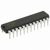
CY7C63743-PXC Cypress Semiconductor Corp, CY7C63743-PXC Datasheet - Page 10

CY7C63743-PXC
Manufacturer Part Number
CY7C63743-PXC
Description
IC MCU 8K USB/PS2 LS 24DIP
Manufacturer
Cypress Semiconductor Corp
Series
enCoRe™r
Specifications of CY7C63743-PXC
Applications
USB Microcontroller
Core Processor
M8B
Program Memory Type
OTP (8 kB)
Controller Series
CY7C637xx
Ram Size
256 x 8
Interface
PS2, USB
Number Of I /o
16
Voltage - Supply
4 V ~ 5.5 V
Operating Temperature
0°C ~ 70°C
Mounting Type
Through Hole
Package / Case
24-DIP (0.300", 7.62mm)
Lead Free Status / RoHS Status
Lead free / RoHS Compliant
Other names
428-1621
Available stocks
Company
Part Number
Manufacturer
Quantity
Price
Company:
Part Number:
CY7C63743-PXC
Manufacturer:
TI
Quantity:
12 749
Clocking
The chip can be clocked from either the internal on-chip clock, or from an oscillator based on an external resonator/crystal, as shown
in
Register,
Bit 7: Ext. Clock Resume Delay
Document #: 38-08022 Rev. *D
Figure
External Clock Resume Delay bit selects the delay time when
switching to the external oscillator from the internal oscillator
mode, or when waking from suspend mode with the external
oscillator enabled.
1 = 4 ms delay.
0 = 128 μs delay.
The delay gives the oscillator time to start up. The shorter time
is adequate for operation with ceramic resonators, while the
longer time is preferred for start-up with a crystal. (These
times do not include an initial oscillator start-up time which
depends on the resonating element. This time is typically
50–100 μs for ceramic resonators and 1–10 ms for crystals).
Note that this bit only selects the delay time for the external
clock mode. When waking from suspend mode with the inter-
nal oscillator (Bit 0 is LOW), the delay time is only 8 μs in
Read/Write
Bit Name
Reset
Bit #
. No additional capacitance is included on chip at the XTALIN/OUT pins. Operation is controlled by the Clock Configuration
Figure
(to Microcontroller)
Clk2x (12 MHz)
Clk1x (6 MHz)
(to USB SIE)
.
Int Clk Output Disable
Ext. Clock
Resume
Ext Clk Enable
Delay
R/W
7
0
Internal Osc
Port 2.1
R/W
Figure 4. Clock Configuration Register (Address 0xF8)
Wake-up Timer Adjust Bit [2:0]
6
0
Doubler
Clock
Figure 3. Clock Oscillator On-chip Circuit
R/W
5
0
R/W
4
0
Bit [6:4]: Wake-up Timer Adjust Bit [2:0]
addition to a delay of approximately 1 μs for the oscillator to
start.
The Wake-up Timer Adjust Bits are used to adjust the
Wake-up timer period.
If the Wake-up interrupt is enabled in the Global Interrupt En-
able Register, the microcontroller will generate wake-up inter-
rupts periodically. The frequency of these periodical wake-up
interrupts is adjusted by setting the Wake-up Timer Adjust Bit
[2:0], as described in Section . One common use of the
wake-up interrupts is to generate periodical wake-up events
during suspend mode to check for changes, such as looking
for movement in a mouse, while maintaining a low average
power.
Low-voltage
Disable
Reset
R/W
3
0
Precision
Clocking
Enable
USB
R/W
2
0
Internal
Disable
Output
Clock
R/W
1
0
CY7C63722C
CY7C63723C
CY7C63743C
XTALOUT
XTALIN
Oscillator
Page 10 of 53
External
Enable
R/W
0
0
[+] Feedback


