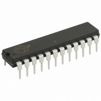
CY7C63743-PXC Cypress Semiconductor Corp, CY7C63743-PXC Datasheet - Page 31

CY7C63743-PXC
Manufacturer Part Number
CY7C63743-PXC
Description
IC MCU 8K USB/PS2 LS 24DIP
Manufacturer
Cypress Semiconductor Corp
Series
enCoRe™r
Specifications of CY7C63743-PXC
Applications
USB Microcontroller
Core Processor
M8B
Program Memory Type
OTP (8 kB)
Controller Series
CY7C637xx
Ram Size
256 x 8
Interface
PS2, USB
Number Of I /o
16
Voltage - Supply
4 V ~ 5.5 V
Operating Temperature
0°C ~ 70°C
Mounting Type
Through Hole
Package / Case
24-DIP (0.300", 7.62mm)
Lead Free Status / RoHS Status
Lead free / RoHS Compliant
Other names
428-1621
Available stocks
Company
Part Number
Manufacturer
Quantity
Price
Company:
Part Number:
CY7C63743-PXC
Manufacturer:
TI
Quantity:
12 749
Interrupt Sources
The following sections provide details on the different types of interrupt sources.
Bit 7: Wake-up Interrupt Enable
Bit 6: GPIO Interrupt Enable
Document #: 38-08022 Rev. *D
Read/Write
Bit Name
The internal wake-up timer is normally used to wake the part
from suspend mode, but it can also provide an interrupt when
the part is awake. The wake-up timer is cleared whenever the
Wake-up Interrupt Enable bit is written to a 0, and runs when-
ever that bit is written to a 1. When the interrupt is enabled,
the wake-up timer provides periodic interrupts at multiples of
period, as described in Section .
1 = Enable wake-up timer for periodic wake-up.
0 = Disable and power-off wake-up timer.
Each GPIO pin can serve as an interrupt input. During a reset,
GPIO interrupts are disabled by clearing all GPIO interrupt
enable registers. Writing a ‘1’ to a GPIO Interrupt Enable bit
enables GPIO interrupts from the corresponding input pin.
These registers are shown in Figure 37 for Port 0 and
Figure 38 for Port 1. In addition to enabling the desired indi-
vidual pins for interrupt, the main GPIO interrupt must be en-
abled, as explained in Section .
The polarity that triggers an interrupt is controlled indepen-
dently for each GPIO pin by the GPIO Interrupt Polarity Reg-
isters. Setting a Polarity bit to ‘0’ allows an interrupt on a falling
GPIO edge, while setting a Polarity bit to ‘1’ allows an interrupt
on a rising GPIO edge. The Polarity Registers reset to 0 and
are shown in Figure 39 for Port 0 and Figure for Port 1.
All of the GPIO pins share a single interrupt vector, which
means the firmware will need to read the GPIO ports with
enabled interrupts to determine which pin or pins caused an
interrupt.The GPIO interrupt structure is illustrated in Figure .
Note that if one port pin triggered an interrupt, no other port
pins can cause a GPIO interrupt until that port pin has re-
turned to its inactive (non-trigger) state or its corresponding
port interrupt enable bit is cleared. The CY7C637xxC does
not assign interrupt priority to different port pins and the Port
Interrupt Enable Registers are not affected by the interrupt
acknowledge process.
1 = Enable
0 = Disable
Reset
Bit #
Wake-up
Interrupt
Enable
R/W
7
0
Interrupt
Enable
GPIO
R/W
Figure 34. Global Interrupt Enable Register (Address 0x20)
6
0
Intr. Enable
Capture
Timer B
R/W
5
0
Intr. Enable
Capture
Timer A
R/W
4
0
Bit [5:4]: Capture Timer A and B Interrupts
There are two capture timer interrupts, one for each associated
pin. Each of these interrupts occurs on an enabled edge of the
selected GPIO pin(s). For each pin, rising and/or falling edge
capture interrupts can be in selected. Refer to Section . These
interrupts are independent of the GPIO interrupt, described in the
next section.
Bit 3: SPI Interrupt Enable
The SPI interrupt occurs at the end of each SPI byte transaction,
at the final clock edge, as shown in Figure 23. After the interrupt,
the received data byte can be read from the SPI Data Register,
and the TCMP control bit will be high
Bit 2: 1.024-ms Interrupt Enable
Bit 1: 128-μs Interrupt Enable
1 = Enable
0 = Disable
1 = Enable
0 = Disable
The 1.024-ms interrupts are periodic timer interrupts from the
free-running timer (based on the 6-MHz clock). The user
should disable this interrupt before going into the suspend
mode to avoid possible conflicts between servicing the timer
interrupts (128-μs interrupt and 1.024-ms interrupt) first or the
suspend request first when waking up.
1 = Enable. Periodic interrupts will be generated approximate-
ly every 1.024 ms.
0 = Disable.
The 128-μs interrupt is another source of timer interrupt from
the free-running timer. The user should disable both timer in-
terrupts (128-μs and 1.024-ms) before going into the suspend
mode to avoid possible conflicts between servicing the timer
interrupts first or the suspend request first when waking up.
1 = Enable. Periodic interrupts will be generated approximate-
ly every 128 μs.
0 = Disable.
Interrupt
Enable
R/W
SPI
3
0
1.024-ms
Interrupt
Enable
R/W
2
0
Interrupt
128-μs
Enable
R/W
1
0
CY7C63722C
CY7C63723C
CY7C63743C
PS/2 Activity
Intr. Enable
USB Bus
Reset /
Page 31 of 53
R/W
0
0
[+] Feedback


