CY7C64714-56PVXC Cypress Semiconductor Corp, CY7C64714-56PVXC Datasheet - Page 31
CY7C64714-56PVXC
Manufacturer Part Number
CY7C64714-56PVXC
Description
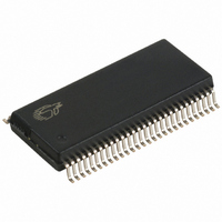
IC MCU USB EZ FX1 16KB 56-SSOP
Manufacturer
Cypress Semiconductor Corp
Series
EZ-USB FX1™r
Datasheet
1.CY7C64714-100AXC.pdf
(50 pages)
Specifications of CY7C64714-56PVXC
Applications
USB Microcontroller
Core Processor
8051
Program Memory Type
ROMless
Controller Series
CY7C647xx
Ram Size
16K x 8
Interface
I²C, USB, USART
Number Of I /o
24
Voltage - Supply
3.15 V ~ 3.45 V
Operating Temperature
0°C ~ 70°C
Mounting Type
Surface Mount
Package / Case
56-SSOP
Lead Free Status / RoHS Status
Lead free / RoHS Compliant


10.3
Table 10-2. Data Memory Read Parameters
Document #: 38-08039 Rev. *C
t
t
t
t
t
t
t
t
When using the AUTPOPTR1 or AUTOPTR2 to address external memory, the address of AUTOPTR1 will only be active while
either RD# or WR# are active. The address of AUTOPTR2 will be active throughout the cycle and meet the above address valid
time for which is based on the stretch value.
Note:
16. t
CL
AV
STBL
STBH
SCSL
SOEL
DSU
DH
Parameter
t
t
t
t
ACC2
ACC2
ACC2
ACC3
ACC3
CLKOUT
Data Memory Read
(24 MHz) = 3*t
(48 MHz) = 3*t
(24 MHz) = 5*t
(48 MHz) = 5*t
CLKOUT
and t
ACC3
A[15..0]
A[15..0]
[14]
D[7..0]
D[7..0]
are computed from the above parameters as follows:
[14]
1/CLKOUT Frequency
Delay from Clock to Valid Address
Clock to RD LOW
Clock to RD HIGH
Clock to CS LOW
Clock to OE LOW
Data Setup to Clock
Data Hold Time
OE#
RD#
RD#
CS#
CS#
CL
CL
CL
CL
– t
– t
– t
– t
AV
AV
AV
AV
– t
– t
– t
– t
DSU
DSU
DSU
DSU
t
t
AV
AV
t
t
CL
CL
= 106 ns
= 43 ns
= 190 ns
= 86 ns.
Description
Figure 10-2. Data Memory Read Timing Diagram
t
STBL
t
t
ACC1
SCSL
t
SOEL
[16
Stretch = 0
Stretch = 1
t
data in
DSU
t
ACC1
Min.
[16]
9.6
t
0
STBH
t
DH
20.83
41.66
Typ.
83.2
t
AV
t
data in
DSU
Max.
10.7
11.1
13
11
11
t
DH
CY7C64713/14
Unit
ns
ns
ns
ns
ns
ns
ns
ns
ns
ns
Page 31 of 50
48 MHz
24 MHz
12 MHz
Notes
Related parts for CY7C64714-56PVXC
Image
Part Number
Description
Manufacturer
Datasheet
Request
R

Part Number:
Description:
IC MCU USB EZ FX1 16KB 100LQFP
Manufacturer:
Cypress Semiconductor Corp
Datasheet:

Part Number:
Description:
IC MCU USB EZ FX1 16KB 128LQFP
Manufacturer:
Cypress Semiconductor Corp
Datasheet:
Part Number:
Description:
IC MCU USB EZ FX1 16KB 56VQFN
Manufacturer:
Cypress Semiconductor Corp
Datasheet:
Part Number:
Description:
Manufacturer:
Cypress Semiconductor Corp
Datasheet:
Part Number:
Description:
Manufacturer:
Cypress Semiconductor Corp
Datasheet:
Part Number:
Description:
Manufacturer:
Cypress Semiconductor Corp
Datasheet:
Part Number:
Description:
Manufacturer:
Cypress Semiconductor Corp
Datasheet: