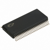
CY7C64714-56PVXC Cypress Semiconductor Corp, CY7C64714-56PVXC Datasheet - Page 45

CY7C64714-56PVXC
Manufacturer Part Number
CY7C64714-56PVXC
Description
IC MCU USB EZ FX1 16KB 56-SSOP
Manufacturer
Cypress Semiconductor Corp
Series
EZ-USB FX1™r
Datasheet
1.CY7C64714-100AXC.pdf
(50 pages)
Specifications of CY7C64714-56PVXC
Applications
USB Microcontroller
Core Processor
8051
Program Memory Type
ROMless
Controller Series
CY7C647xx
Ram Size
16K x 8
Interface
I²C, USB, USART
Number Of I /o
24
Voltage - Supply
3.15 V ~ 3.45 V
Operating Temperature
0°C ~ 70°C
Mounting Type
Surface Mount
Package / Case
56-SSOP
Lead Free Status / RoHS Status
Lead free / RoHS Compliant
10.17.4 Sequence Diagram of a Single and Burst Asynchronous Write
Figure 10-23 diagrams the timing relationship of the SLAVE
FIFO write in an asynchronous mode. The diagram shows a
single write followed by a burst write of 3 bytes and committing
the 4-byte-short packet using PKTEND.
11.0
Table 11-1. Ordering Information
Document #: 38-08039 Rev. *C
Ideal for battery powered applications
CY7C64714-128AXC
CY7C64714-100AXC
CY7C64714-56LFXC
Ideal for non-battery powered applications
CY7C64713-128AXC
CY7C64713-100AXC
CY7C64713-56LFXC
CY3674
FIFOADR
PKTEND
• At t = 0 the FIFO address is applied, insuring that it meets
• At t = 1 SLWR is asserted. SLWR must meet the minimum
• At t = 2, data must be present on the bus t
• At t = 3, deasserting SLWR will cause the data to be written
FLAGS
SLWR
the setup time of t
asserted (SLCS may be tied low in some applications).
active pulse of t
of t
SLWR or before SLWR is asserted.
deasserting edge of SLWR.
from the data bus to the FIFO and then increments the FIFO
DATA
SLCS
WRpwh
Ordering Code
Ordering Information
. If the SLCS is used, it must be in asserted with
t=0
t
SFA
WRpwl
t =1
SFA
t
Figure 10-23. Slave FIFO Asynchronous Write Sequence and Timing Diagram
WRpwl
t=2
t
SFD
. If SLCS is used, it must also be
and minimum de-active pulse width
t=3
N
t
t
FDH
WRpwh
t
FAH
t
XFLG
128 TQFP – Lead-Free
100 TQFP – Lead-Free
56 QFN – Lead-Free
128 TQFP - Lead-Free
100 TQFP - Lead-Free
56 QFN - Lead-Free
EZ-USB FX1 Development Kit
T=0
SFD
t
SFA
Package Type
T=1
before the
t
WRpwl
T=2
t
SFD
T=3
t
N+1
FDH
t
WRpwh
T=4
The same sequence of events are shown for a burst write and
is indicated by the timing marks of T = 0 through 5. Note: In
the burst write mode, once SLWR is deasserted, the data is
written to the FIFO and then the FIFO pointer is incremented
to the next byte in the FIFO. The FIFO pointer is post incre-
mented.
In Figure 10-23, once the four bytes are written to the FIFO
and SLWR is deasserted, the short 4-byte packet can be
committed to the host using the PKTEND. The external device
should be designed to not assert SLWR and the PKTEND
signal at the same time. It should be designed to assert the
PKTEND after SLWR is deasserted and met the minimum
deasserted pulse width. The FIFOADDR lines are to be held
constant during the PKTEND assertion.
t
WRpwl
T=5
pointer. The FIFO flag is also updated after t
de-asserting edge of SLWR.
t
SFD
T=6
t
N+2
FDH
t
WRpwh
T=7
RAM Size
t
WRpwl
16K
16K
16K
16K
16K
16K
T=8
t
SFD
T=9
t
t
N+3
WRpwh
FDH
# Prog I/Os
40
40
24
40
40
24
CY7C64713/14
t
PEpwl
[17]
t
XFLG
t
/Data Busses
PEpwh
t
FAH
XFLG
Page 45 of 50
Address
16/8 bit
16/8 bit
8051
–
–
-
-
from the


