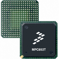
MPC852TVR50A Freescale Semiconductor, MPC852TVR50A Datasheet - Page 9

MPC852TVR50A
Manufacturer Part Number
MPC852TVR50A
Description
IC MPU POWERQUICC 50MHZ 256PBGA
Manufacturer
Freescale Semiconductor
Series
PowerQUICC Ir
Datasheet
1.MPC852TVR50A.pdf
(80 pages)
Specifications of MPC852TVR50A
Processor Type
MPC8xx PowerQUICC 32-Bit
Speed
50MHz
Voltage
1.8V
Mounting Type
Surface Mount
Package / Case
256-PBGA
Processor Series
MPC8xx
Core
MPC8xx
Data Bus Width
32 bit
Development Tools By Supplier
MPC852TADS-KIT
Maximum Clock Frequency
50 MHz
Operating Supply Voltage
0 V to 3.3 V
Maximum Operating Temperature
+ 105 C
Mounting Style
SMD/SMT
Data Ram Size
8 KB
I/o Voltage
3.3 V
Interface Type
SPI, UART
Minimum Operating Temperature
0 C
Program Memory Size
4 KB
Program Memory Type
EPROM/Flash
Core Size
32 Bit
Cpu Speed
50MHz
Embedded Interface Type
SPI
Digital Ic Case Style
BGA
No. Of Pins
256
Rohs Compliant
Yes
Lead Free Status / RoHS Status
Lead free / RoHS Compliant
Features
-
Lead Free Status / Rohs Status
Lead free / RoHS Compliant
Available stocks
Company
Part Number
Manufacturer
Quantity
Price
Company:
Part Number:
MPC852TVR50A
Manufacturer:
FREESCALE
Quantity:
662
Company:
Part Number:
MPC852TVR50A
Manufacturer:
FREESCAL
Quantity:
319
Company:
Part Number:
MPC852TVR50A
Manufacturer:
Freescale Semiconductor
Quantity:
10 000
Part Number:
MPC852TVR50A
Manufacturer:
FREESCALE
Quantity:
20 000
1
2
3
4
7
For the following discussions, P
drivers.
7.1
An estimation of the chip junction temperature, T
Freescale Semiconductor
Input leakage current, Vin = 5.5 V (Except TMS, TRST,
DSCK and DSDI pins) for 5-V tolerant pins
Input leakage current, Vin = V
DSCK, and DSDI)
Input leakage current, Vin = 0 V (Except TMS, TRST,
DSCK and DSDI pins)
Input capacitance
Output high voltage, IOH = -2.0 mA, V
Except XTAL and open drain pins
Output low voltage
IOL = 2.0 mA (CLKOUT)
IOL = 3.2 mA
IOL = 5.3 mA
IOL = 7.0 mA (Txd1/pa14, txd2/pa12)
IOL = 8.9 mA (TS, TA, TEA, BI, BB, HRESET, SRESET)
The PA[0:3], PA[8:11], PB15, PB[24:25]; PB[28:31], PC[4:7], PC[12:13], PC15, PD[3:15], TDI, TDO, TCK, TRST, TMS,
MII_TXEN, MII_MDIO are 5-V tolerant pins.
Input capacitance is periodically sampled.
A(0:31), TSIZ0/REG, TSIZ1, D(0:31), DP(0:3)/IRQ(3:6), RD/WR, BURST, RSV/IRQ2, IWP(0:1)/VFLS(0:1), RXD3/PA11,
TXD3/PA10, RXD4/PA9, TXD4/PA8, TIN3/BRGO3/CLK5/PA3, BRGCLK2/TOUT3/CLK6/PA2, TIN4/BRGO4/CLK7/PA1,
TOUT4/CLK8/PA0, SPISEL/PB31, SPICLK/PB30, SPIMOSI/PB29, BRGO4/SPIMISO/PB28, SMTXD1/PB25,
SMRXD1/PB24, BRGO3/PB15, RTS1/DREQ0/PC15, RTS3/PC13, RTS4/PC12, CTS3/PC7, CD3/PC6, CTS4/SDACK1/PC5,
CD4/PC4, MII-RXD3/PD15, MII-RXD2/PD14, MII-RXD1/PD13, MII-MDC/PD12, MII-TXERR/RXD3/PD11,
MII-RX0/TXD3/PD10, MII-TXD0/RXD4/PD9, MII-RXCLK/TXD4/PD8, MII-TXD3/PD5, MII-RXDV/RTS4/PD6,
MII-RXERR/RTS3/PD7, MII-TXD2/REJECT3/PD4, MII-TXD1/REJECT4/PD3, MII_CRS, MII_MDIO, MII_TXEN, and MII_COL
BDIP/GPL_B(5), BR, BG, FRZ/IRQ6, CS(0:5), CS(6), CS(7), WE0/BS_B0/IORD, WE1/BS_B1/IOWR, WE2/BS_B2/PCOE,
WE3/ BS_B3/PCWE, BS_A(0:3), GPL_A0/GPL_B0, OE/GPL_A1/GPL_B1, GPL_A(2:3)/GPL_B(2:3)/CS(2:3),
UPWAITA/GPL_A4, GPL_A5, ALE_A, CE1_A, CE2_A, DSCK, OP(0:1), OP2/MODCK1/STS, OP3/MODCK2/DSDO, and
BADDR(28:30)
Thermal Calculation and Measurement
Estimation with Junction-to-Ambient Thermal Resistance
3
4
T
2
J
= T
Characteristic
A
+(R
DDH
θJA
MPC852T PowerQUICC™ Hardware Specifications, Rev. 4
Table 5. DC Electrical Specifications (continued)
(Except TMS, TRST,
The V
× P
D
DDH
= (V
D
)
= 3.0 V
1
DDSYN
DDL
x IDDL) + P
power dissipation is negligible.
J
NOTE
, in °C can be obtained from the equation:
Symbol
I/O
VOH
VOL
C
I
I
I
, where P
in
In
In
in
I/O
is the power dissipation of the I/O
Min
Thermal Calculation and Measurement
2.4
—
—
—
—
—
Max
100
0.5
10
10
20
—
Unit
µA
µA
µA
pF
V
V
9


