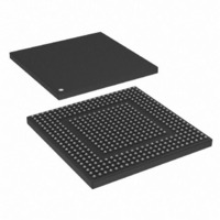
MPC8308VMAGD Freescale Semiconductor, MPC8308VMAGD Datasheet - Page 25

MPC8308VMAGD
Manufacturer Part Number
MPC8308VMAGD
Description
MPU POWERQUICC II PRO 473MAPBGA
Manufacturer
Freescale Semiconductor
Datasheets
1.MPC8308VMAGD.pdf
(90 pages)
2.MPC8308VMAGD.pdf
(2 pages)
3.MPC8308VMAGD.pdf
(1170 pages)
4.MPC8308VMAGD.pdf
(14 pages)
Specifications of MPC8308VMAGD
Processor Type
MPC83xx PowerQUICC II Pro 32-Bit
Speed
400MHz
Voltage
1V
Mounting Type
Surface Mount
Package / Case
473-MAPBGA
Product
Network Processor
Data Rate
256 bps
Frequency
400 MHz
Supply Voltage (max)
3.6 V
Supply Voltage (min)
3 V
Supply Current (max)
5 uA
Maximum Operating Temperature
+ 105 C
Minimum Operating Temperature
0 C
Interface
I2C, JTAG, SPI
Mounting Style
SMD/SMT
Lead Free Status / RoHS Status
Lead free / RoHS Compliant
Features
-
Lead Free Status / Rohs Status
Lead free / RoHS Compliant
Available stocks
Company
Part Number
Manufacturer
Quantity
Price
Company:
Part Number:
MPC8308VMAGD
Manufacturer:
FREESCAL
Quantity:
300
Company:
Part Number:
MPC8308VMAGD
Manufacturer:
Freescale Semiconductor
Quantity:
10 000
Part Number:
MPC8308VMAGD
Manufacturer:
FREESCALE
Quantity:
20 000
Company:
Part Number:
MPC8308VMAGD400/266
Manufacturer:
FREESCAL
Quantity:
300
Company:
Part Number:
MPC8308VMAGDA
Manufacturer:
Freescale Semiconductor
Quantity:
10 000
10 High-Speed Serial Interfaces (HSSI)
This section describes the common portion of SerDes DC electrical specifications, which is the DC
requirement for SerDes reference clocks. The SerDes data lane’s transmitter and receiver reference circuits
are also shown.
10.1
The SerDes utilizes differential signaling to transfer data across the serial link. This section defines terms
used in the description and specification of differential signals.
Figure 15
description. The figure shows waveform for either a transmitter output (TXn and TXn) or a receiver input
(RXn and RXn). Each signal swings between A Volts and B Volts where A > B.
Using this waveform, the definitions are as follows. To simplify illustration, the following definitions
assume that the SerDes transmitter and receiver operate in a fully symmetrical differential signaling
environment.
Freescale Semiconductor
•
•
•
•
•
•
Single-Ended Swing
The transmitter output signals and the receiver input signals TXn, TXn, RXn and RXn each have
a peak-to-peak swing of A – B Volts. This is also referred as each signal wire’s single-ended swing.
Differential Output Voltage, V
The differential output voltage (or swing) of the transmitter, V
the two complimentary output voltages: V
negative.
Differential Input Voltage, V
The differential input voltage (or swing) of the receiver, V
complimentary input voltages: V
Differential Peak Voltage, V
The peak value of the differential transmitter output signal or the differential receiver input signal
is defined as Differential Peak Voltage, V
Differential Peak-to-Peak, V
Since the differential output signal of the transmitter and the differential input signal of the receiver
each range from A – B to –(A – B) Volts, the peak-to-peak value of the differential transmitter
output signal or the differential receiver input signal is defined as differential peak-to-peak voltage,
V
twice of the differential peak. For example, the output differential peak-peak voltage can also be
calculated as V
Differential Waveform
The differential waveform is constructed by subtracting the inverting signal (for example, TXn)
from the non-inverting signal (for example, TXn) within a differential pair. There is only one signal
trace curve in a differential waveform. The voltage represented in the differential waveform is not
referenced to ground. Refer to
DIFFp-p
Signal Terms Definition
shows how the signals are defined. For illustration purpose, only one SerDes lane is used for
= 2*V
MPC8308 PowerQUICC II Pro Processor Hardware Specification, Rev. 2
TX-DIFFp-p
DIFFp
= 2 * |(A – B)| Volts, which is twice of differential swing in amplitude, or
= 2*|V
DIFFp
DIFFp-p
ID
Figure 24
OD
RXn
OD
(or Differential Input Swing)
(or Differential Output Swing)
|.
– V
RXn
as an example for differential waveform.
DIFFp
TXn
. The V
– V
= |A – B| Volts.
TXn
ID
. The V
value can be either positive or negative.
ID
, is defined as the difference of the two
OD
OD
value can be either positive or
, is defined as the difference of
High-Speed Serial Interfaces (HSSI)
25


