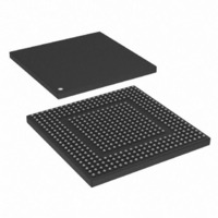
MPC8308VMAGD Freescale Semiconductor, MPC8308VMAGD Datasheet - Page 43

MPC8308VMAGD
Manufacturer Part Number
MPC8308VMAGD
Description
MPU POWERQUICC II PRO 473MAPBGA
Manufacturer
Freescale Semiconductor
Datasheets
1.MPC8308VMAGD.pdf
(90 pages)
2.MPC8308VMAGD.pdf
(2 pages)
3.MPC8308VMAGD.pdf
(1170 pages)
4.MPC8308VMAGD.pdf
(14 pages)
Specifications of MPC8308VMAGD
Processor Type
MPC83xx PowerQUICC II Pro 32-Bit
Speed
400MHz
Voltage
1V
Mounting Type
Surface Mount
Package / Case
473-MAPBGA
Product
Network Processor
Data Rate
256 bps
Frequency
400 MHz
Supply Voltage (max)
3.6 V
Supply Voltage (min)
3 V
Supply Current (max)
5 uA
Maximum Operating Temperature
+ 105 C
Minimum Operating Temperature
0 C
Interface
I2C, JTAG, SPI
Mounting Style
SMD/SMT
Lead Free Status / RoHS Status
Lead free / RoHS Compliant
Features
-
Lead Free Status / Rohs Status
Lead free / RoHS Compliant
Available stocks
Company
Part Number
Manufacturer
Quantity
Price
Company:
Part Number:
MPC8308VMAGD
Manufacturer:
FREESCAL
Quantity:
300
Company:
Part Number:
MPC8308VMAGD
Manufacturer:
Freescale Semiconductor
Quantity:
10 000
Part Number:
MPC8308VMAGD
Manufacturer:
FREESCALE
Quantity:
20 000
Company:
Part Number:
MPC8308VMAGD400/266
Manufacturer:
FREESCAL
Quantity:
300
Company:
Part Number:
MPC8308VMAGDA
Manufacturer:
Freescale Semiconductor
Quantity:
10 000
and silicon. The RX eye diagram must be aligned in time using the jitter median to locate the center of the
eye diagram.
The eye diagram must be valid for any 250 consecutive UIs.
A recovered TX UI is calculated over 3500 consecutive unit intervals of sample data. The eye diagram is
created using all edges of the 250 consecutive UI in the center of the 3500 UI used for calculating the TX
UI.
11.5.1
The AC timing and voltage parameters must be verified at the measurement point, as specified within
0.2 inches of the package pins, into a test/measurement load shown in
Freescale Semiconductor
Compliance Test and Measurement Load
Figure 28. Minimum Receiver Eye Timing and Voltage Compliance Specification
The reference impedance for return loss measurements is 50 Ω to ground for
both the D+ and D- line (that is, as measured by a Vector Network Analyzer
with 50 Ω probes—see
C
The allowance of the measurement point to be within 0.2 inches of the
package pins is meant to acknowledge that package/board routing may
benefit from D+ and D– not being exactly matched in length at the package
pin boundary.
PEACCTX
MPC8308 PowerQUICC II Pro Processor Hardware Specification, Rev. 2
(D+ D– Crossing Point)
V
RX-DIFF
, are optional for the return loss measurement.
= 0 mV
Figure
V
RX-DIFFp-p-MIN
0.4 UI = T
29). Note that the series capacitors,
NOTE
NOTE
RX-EYE-MIN
> 175 mV
(D+ D– Crossing Point)
V
RX-DIFF
Figure
= 0 mV
29.
PCI Express
43


