MPC8308VMAGD Freescale Semiconductor, MPC8308VMAGD Datasheet - Page 8
MPC8308VMAGD
Manufacturer Part Number
MPC8308VMAGD
Description
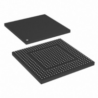
MPU POWERQUICC II PRO 473MAPBGA
Manufacturer
Freescale Semiconductor
Datasheets
1.MPC8308VMAGD.pdf
(90 pages)
2.MPC8308VMAGD.pdf
(2 pages)
3.MPC8308VMAGD.pdf
(1170 pages)
4.MPC8308VMAGD.pdf
(14 pages)
Specifications of MPC8308VMAGD
Processor Type
MPC83xx PowerQUICC II Pro 32-Bit
Speed
400MHz
Voltage
1V
Mounting Type
Surface Mount
Package / Case
473-MAPBGA
Product
Network Processor
Data Rate
256 bps
Frequency
400 MHz
Supply Voltage (max)
3.6 V
Supply Voltage (min)
3 V
Supply Current (max)
5 uA
Maximum Operating Temperature
+ 105 C
Minimum Operating Temperature
0 C
Interface
I2C, JTAG, SPI
Mounting Style
SMD/SMT
Lead Free Status / RoHS Status
Lead free / RoHS Compliant
Features
-
Lead Free Status / Rohs Status
Lead free / RoHS Compliant
Available stocks
Company
Part Number
Manufacturer
Quantity
Price
Company:

Part Number:
MPC8308VMAGD
Manufacturer:
FREESCAL
Quantity:
300
Company:
Part Number:
MPC8308VMAGD
Manufacturer:
Freescale Semiconductor
Quantity:
10 000
Part Number:
MPC8308VMAGD
Manufacturer:
FREESCALE
Quantity:
20 000
Company:
Part Number:
MPC8308VMAGD400/266
Manufacturer:
FREESCAL
Quantity:
300
Company:
Part Number:
MPC8308VMAGDA
Manufacturer:
Freescale Semiconductor
Quantity:
10 000


RESET Initialization
4.2
The primary clock source for the device is SYS_CLK_IN.
(SYS_CLK_IN) AC timing specifications for the device.
5
This section describes the DC and AC electrical specifications for the reset initialization timing and
electrical requirements of the device.
5.1
Table 10
8
RTC_PIT_CLOCK frequency
RTC_PIT_CLOCK rise and fall time
RTC_PIT_CLOCK duty cycle
SYS_CLK_IN frequency
SYS_CLK_IN period
SYS_CLK_IN rise and fall time
SYS_CLK_IN duty cycle
SYS_CLK_IN jitter
Notes:
1. Caution: The system and core must not exceed their respective maximum or minimum operating frequencies.
2. Rise and fall times for SYS_CLK_IN are measured at 0.4 and 2.7 V.
3. Timing is guaranteed by design and characterization.
4. This represents the total input jitter—short term and long term—and is guaranteed by design.
5. The SYS_CLK_IN driver’s closed loop jitter bandwidth should be <500 kHz at –20 dB. The bandwidth must be set low to
6. Spread spectrum is allowed up to 1% down-spread @ 33 kHz (max rate).
allow cascade-connected PLL-based devices to track SYS_CLK_IN drivers with the specified jitter.
RESET Initialization
provides the DC electrical characteristics for the RESET pins.
AC Electrical Characteristics
RESET DC Electrical Characteristics
Parameter/
Input high voltage
Input low voltage
Input current
Output high voltage
Parameter/
Characteristic
MPC8308 PowerQUICC II Pro Processor Hardware Specification, Rev. 2
Table 9. RTC_PIT_CLOCK AC Timing Specifications
Table 10. RESET Pins DC Electrical Characteristics
Table 8. SYS_CLK_IN AC Timing Specifications
Symbol
V
V
t
V
I
RTCHK
IN
OH
IH
IL
f
RTC_PIT_CLOCK
t
t
KHK
RTCH
Symbol
f
t
SYS_CLK_IN
SYS_CLK_IN
/t
Symbol
/t
RTC_PIT_CLO
t
KH
CK
SYS_CLK_IN
0 V ≤ V
, t
—
, t
RTCL
I
OH
KL
Condition
= –8.0 mA
IN
—
—
≤ NV
Table 8
Min
0.6
Min
DD
24
15
40
1.5
—
45
1
–0.3
Min
2.0
2.4
provides the system clock input
32768
Typ
Typ
—
—
—
—
—
—
NV
DD
Max
0.8
±5
—
66.67
41.67
±150
Max
+ 0.3
Max
1.2
60
55
—
3
Freescale Semiconductor
Unit
μA
V
V
V
MHz
Unit
Unit
ns
ns
ps
%
Hz
μs
%
Notes
Notes
1, 6
4, 5
—
—
—
—
2
3
Related parts for MPC8308VMAGD
Image
Part Number
Description
Manufacturer
Datasheet
Request
R

Part Number:
Description:
Development Boards & Kits - Other Processors MPC8308-NSG
Manufacturer:
Freescale Semiconductor
Datasheet:

Part Number:
Description:
MCU, MPU & DSP Development Tools For MPC8308 Ethernet USB I2C SPI
Manufacturer:
Freescale Semiconductor
Datasheet:
Part Number:
Description:
MCU, MPU & DSP Development Tools For MPC8308 Ethernet USB 32bit
Manufacturer:
Freescale Semiconductor
Datasheet:

Part Number:
Description:
Mpc8308 Powerquicc Ii Pro Processor Hardware Specification
Manufacturer:
Freescale Semiconductor, Inc
Datasheet:

Part Number:
Description:
BOARD REF DESIGN MPC8308
Manufacturer:
Freescale Semiconductor
Datasheet:

Part Number:
Description:
MPC8308 PowerQUICC II Pro Processor Hardware Specification
Manufacturer:
FREESCALE [Freescale Semiconductor, Inc]
Datasheet:
Part Number:
Description:
Microprocessors - MPU E300 ext tmp Qual266
Manufacturer:
Freescale Semiconductor
Datasheet:
Part Number:
Description:
Microprocessors - MPU E300 ext tmp Qual333
Manufacturer:
Freescale Semiconductor
Datasheet:
Part Number:
Description:
Microprocessors - MPU E300 EXT TEMP PB 400
Manufacturer:
Freescale Semiconductor
Datasheet:
Part Number:
Description:
Microprocessors - MPU E300 MP Pb 266
Manufacturer:
Freescale Semiconductor
Datasheet:
Part Number:
Description:
Microprocessors - MPU E300 MP Pb 400
Manufacturer:
Freescale Semiconductor
Datasheet:
Part Number:
Description:
Microprocessors - MPU E300 MP Pb 333
Manufacturer:
Freescale Semiconductor
Datasheet:
Part Number:
Description:
Manufacturer:
Freescale Semiconductor, Inc
Datasheet:
Part Number:
Description:
Manufacturer:
Freescale Semiconductor, Inc
Datasheet:
Part Number:
Description:
Manufacturer:
Freescale Semiconductor, Inc
Datasheet: