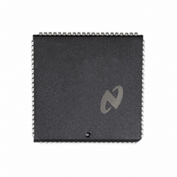
DP8344BV National Semiconductor, DP8344BV Datasheet - Page 10

DP8344BV
Manufacturer Part Number
DP8344BV
Description
IC BIPHASE COMM PROCESSR 84-PLCC
Manufacturer
National Semiconductor
Datasheet
1.DP8344BV.pdf
(184 pages)
Specifications of DP8344BV
Processor Type
8-Bit RISC
Speed
20MHz
Voltage
4.5 ~ 5.5V
Mounting Type
Surface Mount
Package / Case
84-PLCC
Operating Supply Voltage (typ)
5V
Operating Supply Voltage (max)
5.5V
Operating Supply Voltage (min)
4.5V
Mounting
Surface Mount
Operating Temperature (max)
70C
Operating Temperature (min)
0C
Operating Temperature Classification
Commercial
Lead Free Status / RoHS Status
Contains lead / RoHS non-compliant
Features
-
Lead Free Status / Rohs Status
Not Compliant
Other names
*DP8344BV
Available stocks
Company
Part Number
Manufacturer
Quantity
Price
Company:
Part Number:
DP8344BV
Manufacturer:
NSC
Quantity:
5 510
Part Number:
DP8344BV
Manufacturer:
NS/国半
Quantity:
20 000
- Current page: 10 of 184
- Download datasheet (3Mb)
1 0 Communications Processor Introduction
Simultaneous access to both data and program memory
and instruction pipelining greatly enhance the speed per-
formance of the BCP making it well suited for real-time pro-
cessing The pipeline allows the next instruction to be re-
trieved from program memory while the current instruction is
being executed
1 3 TIMING INTRODUCTION
The timing of all CPU operations instruction execution and
memory access is related to the CPU clock This clock is
usually generated by a crystal and the internal oscillator
with optional divide by two circuitry The period of the result-
ing CPU clock is referred to as a T-state for example a
20 MHz CPU clock yields a 50 ns T-state Most CPU func-
tions such as arithmetic and logical operations shifts and
FIGURE 1-5 Effect of Memory Wait States on Timing
FIGURE 1-4 Memory Configuration
10
rotates and register moves require only two T-states
Branching instructions and data memory accesses require
three to four T-states
Each memory system has a separate programmable num-
ber of wait states to allow the use of slower memory devic-
es Instruction memory wait states are inserted into all in-
structions as shown in Figure 1-5
overall speed of program execution Instruction memory
wait states can also apply when the Remote Interface is
loading a program into instruction memory Data memory
wait states are only inserted into data memory access in-
structions hence there is less degradation in overall pro-
gram execution Refer to the Timing section for detailed ex-
amples of all BCP instruction and data memory timing
(Continued)
TL F 9336 – C1
thus they affect the
TL F 9336 – C2
Related parts for DP8344BV
Image
Part Number
Description
Manufacturer
Datasheet
Request
R

Part Number:
Description:
Biphase Communications Processor?BCP
Manufacturer:
NSC [National Semiconductor]
Datasheet:
Part Number:
Description:
National Semiconductor [8-Bit D/A Converter]
Manufacturer:
National Semiconductor
Datasheet:
Part Number:
Description:
National Semiconductor [Media Coprocessor]
Manufacturer:
National Semiconductor
Datasheet:
Part Number:
Description:
Digitally Controlled Tone and Volume Circuit with Stereo Audio Power Amplifier, Microphone Preamp Stage and National 3D Sound
Manufacturer:
National Semiconductor
Datasheet:
Part Number:
Description:
Digitally Controlled Tone and Volume Circuit with Stereo Audio Power Amplifier, Microphone Preamp Stage and National 3D Sound
Manufacturer:
National Semiconductor
Datasheet:
Part Number:
Description:
AC97 Rev 2 Codec with Sample Rate Conversion and National 3D Sound
Manufacturer:
National Semiconductor
Part Number:
Description:
Manufacturer:
National Semiconductor
Datasheet:
Part Number:
Description:
Manufacturer:
National Semiconductor
Datasheet:
Part Number:
Description:
General Purpose, Low Voltage, Low Power, Rail-to-Rail Output Operational Amplifiers
Manufacturer:
National Semiconductor
Datasheet:
Part Number:
Description:
8-bit 20 MSPS flash A/D converter.
Manufacturer:
National Semiconductor
Datasheet:
Part Number:
Description:
Low Noise Quad Operational Amplifier
Manufacturer:
National Semiconductor
Datasheet:
Part Number:
Description:
Quad Differential Line Receivers
Manufacturer:
National Semiconductor
Datasheet:
Part Number:
Description:
Quad High Speed Trapezoidal? Bus Transceiver
Manufacturer:
National Semiconductor
Datasheet:
Part Number:
Description:
Dual Line Receiver
Manufacturer:
National Semiconductor
Datasheet:


