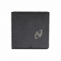
DP8344BV National Semiconductor, DP8344BV Datasheet - Page 149

DP8344BV
Manufacturer Part Number
DP8344BV
Description
IC BIPHASE COMM PROCESSR 84-PLCC
Manufacturer
National Semiconductor
Datasheet
1.DP8344BV.pdf
(184 pages)
Specifications of DP8344BV
Processor Type
8-Bit RISC
Speed
20MHz
Voltage
4.5 ~ 5.5V
Mounting Type
Surface Mount
Package / Case
84-PLCC
Operating Supply Voltage (typ)
5V
Operating Supply Voltage (max)
5.5V
Operating Supply Voltage (min)
4.5V
Mounting
Surface Mount
Operating Temperature (max)
70C
Operating Temperature (min)
0C
Operating Temperature Classification
Commercial
Lead Free Status / RoHS Status
Contains lead / RoHS non-compliant
Features
-
Lead Free Status / Rohs Status
Not Compliant
Other names
*DP8344BV
Available stocks
Company
Part Number
Manufacturer
Quantity
Price
Company:
Part Number:
DP8344BV
Manufacturer:
NSC
Quantity:
5 510
Part Number:
DP8344BV
Manufacturer:
NS/国半
Quantity:
20 000
- Current page: 149 of 184
- Download datasheet (3Mb)
Figure 6-1
6 0 Reference Section
OR OR Immediate
Syntax
OR n rsd
Affected Flags
N Z
Description
Logically ORs the immediate value n to the register rsd and
places the result back into the register rsd Note that only
the active registers R0–R15 may be specified for rsd The
value of n is 8 bits wide
Example
Mask both the Transmitter and Receiver interrupts via the
Interrupt Control Register ICR
rupts unaffected
Instruction Format
T-states
2
Bus Timing
Operation
rsd OR n
0
15
EXX 0 0
OR
Opcode
1
0
00000011B ICR
1
11
rsd
immediate limited register
select main reg banks
mask transmitter and
receiver interrupts
n
R2 Leave the other inter-
(Continued)
3
rsd
0
149
ORA OR with Accumulator
Syntax
ORA Rs Rd
ORA Rs mIr
Affected Flags
N Z
Description
Logically ORs the source register Rs to the active accumu-
lator and places the result into the destination specified
The destination may be either a register Rd or data memo-
ry via an index register mode mIr Note that register bank
selection determines which accumulator is active
Example
Write an 11-bit word to the Transmitter’s FIFO This exam-
ple assumes that the index register IZ points to the location
of the data in memory
Instruction Format
ORA Rs Rd
T-states
ORA Rs Rd
ORA Rs mIr
Bus Timing
ORA Rs Rd
ORA Rs mIr
Operation
ORA Rs Rd
Rs OR accumulator
ORA Rs mIr
Rs OR accumulator
ORA Rs mIr
1
15
TCR settings
EXX
MOVE TCR settings A load accumulator w mask
MOVE
ORA
MOVE
1
Opcode
1
1 1
R20 TCR
IZ
IZ
1
a
a
0
R20
RTR
EQU 00101000B
1
9
Figure 6-1
Figure 6-7
register register
register indexed
2
3
Rd
data memory
select main A alt B
load bits 8 9
write bits 8 9 10 to TCR
push 11-bit word to FIFO
Rd
4
10
TL F 9336 – 11
Rs
0
Related parts for DP8344BV
Image
Part Number
Description
Manufacturer
Datasheet
Request
R

Part Number:
Description:
Biphase Communications Processor?BCP
Manufacturer:
NSC [National Semiconductor]
Datasheet:
Part Number:
Description:
National Semiconductor [8-Bit D/A Converter]
Manufacturer:
National Semiconductor
Datasheet:
Part Number:
Description:
National Semiconductor [Media Coprocessor]
Manufacturer:
National Semiconductor
Datasheet:
Part Number:
Description:
Digitally Controlled Tone and Volume Circuit with Stereo Audio Power Amplifier, Microphone Preamp Stage and National 3D Sound
Manufacturer:
National Semiconductor
Datasheet:
Part Number:
Description:
Digitally Controlled Tone and Volume Circuit with Stereo Audio Power Amplifier, Microphone Preamp Stage and National 3D Sound
Manufacturer:
National Semiconductor
Datasheet:
Part Number:
Description:
AC97 Rev 2 Codec with Sample Rate Conversion and National 3D Sound
Manufacturer:
National Semiconductor
Part Number:
Description:
Manufacturer:
National Semiconductor
Datasheet:
Part Number:
Description:
Manufacturer:
National Semiconductor
Datasheet:
Part Number:
Description:
General Purpose, Low Voltage, Low Power, Rail-to-Rail Output Operational Amplifiers
Manufacturer:
National Semiconductor
Datasheet:
Part Number:
Description:
8-bit 20 MSPS flash A/D converter.
Manufacturer:
National Semiconductor
Datasheet:
Part Number:
Description:
Low Noise Quad Operational Amplifier
Manufacturer:
National Semiconductor
Datasheet:
Part Number:
Description:
Quad Differential Line Receivers
Manufacturer:
National Semiconductor
Datasheet:
Part Number:
Description:
Quad High Speed Trapezoidal? Bus Transceiver
Manufacturer:
National Semiconductor
Datasheet:
Part Number:
Description:
Dual Line Receiver
Manufacturer:
National Semiconductor
Datasheet:


