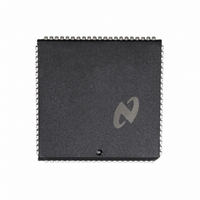
DP8344BV National Semiconductor, DP8344BV Datasheet - Page 45

DP8344BV
Manufacturer Part Number
DP8344BV
Description
IC BIPHASE COMM PROCESSR 84-PLCC
Manufacturer
National Semiconductor
Datasheet
1.DP8344BV.pdf
(184 pages)
Specifications of DP8344BV
Processor Type
8-Bit RISC
Speed
20MHz
Voltage
4.5 ~ 5.5V
Mounting Type
Surface Mount
Package / Case
84-PLCC
Operating Supply Voltage (typ)
5V
Operating Supply Voltage (max)
5.5V
Operating Supply Voltage (min)
4.5V
Mounting
Surface Mount
Operating Temperature (max)
70C
Operating Temperature (min)
0C
Operating Temperature Classification
Commercial
Lead Free Status / RoHS Status
Contains lead / RoHS non-compliant
Features
-
Lead Free Status / Rohs Status
Not Compliant
Other names
*DP8344BV
Available stocks
Company
Part Number
Manufacturer
Quantity
Price
Company:
Part Number:
DP8344BV
Manufacturer:
NSC
Quantity:
5 510
Part Number:
DP8344BV
Manufacturer:
NS/国半
Quantity:
20 000
2-34 The interrupt occurs during the current instruction and
2 0 CPU Description
A call to the interrupt address is generated when an inter-
rupt is detected by the CPU The address for each interrupt
is constructed by concatenating the Interrupt Base Register
in Table 2-28 There is room between the interrupt address-
es for a maximum of four instruction words
Interrupts are sampled by each falling edge of the CPU
clock with the last falling edge prior to the start of the next
instruction determining whether an interrupt will be process-
ed The timing of a typical interrupt event is shown in Figure
is sampled by the falling edge of the CPU clock The next
instruction is not operated on and its address is stored in the
internal address stack along with GIE the ALU flags and
the register bank positions The address stack is twelve
words deep A two T-state internal call is now executed in
place of the non-executed instruction This call will cause a
branch to the interrupt address that is generated in the first
half of T-state T1 Also GIE is cleared at the end of the
first half of T-state T1 The internal call to the interrupt ad-
dress is subject to instruction wait states as configured in
15
IBR
DCR
contents with the individual interrupt code as shown
TABLE 2-28 Interrupt Vector Generation
IBR Contents
NMI
RFF DA RA
TFE
LTA
BIRQ
TO
Interrupt
Interrupt Vector
8
0
(Continued)
0
0
5
Code
Code
111
001
010
011
100
101
FIGURE 2-34 Interrupt Timing
2
0
0
0
45
2-35) the combined circuit forms a Pierce crystal oscillator
2 2 4 Oscillator
The crystal oscillator is an on-chip amplifier which may be
used with an external crystal to generate accurate CPU and
transceiver clocks The input to this amplifier is X1 pin 33
The output of the amplifier is X2 pin 34 When X1 and X2
are connected to a crystal and external capacitors (Figure
with the crystal operating at parallel resonance Crystals
that oscillate over the frequency range of 2 MHz to 20 MHz
may be used The recommended crystal parameters for op-
eration with the oscillator are given in Table 2-29 The exter-
nal capacitor values should be chosen to provide the manu-
facturer’s specified load capacitance for the crystal when
combined with the parasitic capacitance of the trace sock-
et and package As an example a crystal with a specified
load capacitance of 20 pF used in a circuit with 13 pF per
pin parasitic capacitance will require external capacitor val-
ues of 27 pF each This provides an equivalent capacitance
of 40 pF on each side of the crystal and has a 20 pF series
equivalent value across the crystal
As an alternative to the crystal oscillator an external clock
source may be used In this case the external clock source
should be connected to X1 and no external circuitry should
be connected to X2 (Figure 2-36) The DP8344 can supply a
clock source equal in frequency to the crystal oscillator or
external clock source to other circuitry via pin 35 the CLK-
OUT output This output is a buffered version of the signal at
X1
TABLE 2-29 Recommended Crystal Parameters
AT Cut Parallel Resonant
Fundamental Mode
Load Capacitor
Series Resistance
Frequency Tolerance 0 005% at 25 C
Stability 0 01% 0 –70 C
Drive Level 0 5 mW Typical
e
20 pF
k
20
TL F 9336 – F7


