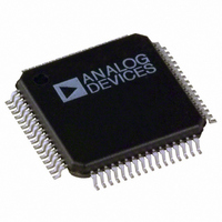
ADV7202KST Analog Devices Inc, ADV7202KST Datasheet - Page 11

ADV7202KST
Manufacturer Part Number
ADV7202KST
Description
IC CODEC VIDEO 10BIT 64LQFP
Manufacturer
Analog Devices Inc
Type
Video Codecr
Datasheet
1.ADV7202KSTZ.pdf
(28 pages)
Specifications of ADV7202KST
Rohs Status
RoHS non-compliant
Data Interface
Serial
Resolution (bits)
12, 10 b
Number Of Adcs / Dacs
1 / 4
Sigma Delta
No
Voltage - Supply, Analog
4.75 V ~ 5.25 V
Voltage - Supply, Digital
4.75 V ~ 5.25 V
Operating Temperature
0°C ~ 70°C
Mounting Type
Surface Mount
Package / Case
64-LQFP
Lead Free Status / Rohs Status
Not Compliant
Available stocks
Company
Part Number
Manufacturer
Quantity
Price
Company:
Part Number:
ADV7202KST
Manufacturer:
CSR
Quantity:
1 000
Company:
Part Number:
ADV7202KSTZ
Manufacturer:
Analog Devices Inc
Quantity:
10 000
VIDEO CLAMPING AND AGC CONTROL
When analog signal clamping is required, the input signal should
be ac-coupled to the input via a capacitor, the clamping control is
via the MPU port. The AGC is implemented digitally. For cor-
rect operation, the user must program the clamp value to which
the signal has been clamped into the ADV7202 I
This allows the user to specify which signal level is unaffected by
the AGC. The digital output signal will be a function of the ADC
output, the AGC Gain, and the Clamp Level and can be repre-
sented as follows:
D
to 2 and can have a value between 0 to 7.99. The Clamp Level is a
10-bit number (0–1023) equal to the 7-bit I
(Clamp Level CR06-CR00); the ADC value can be regarded as
a 10-bit number (0–1023) for the equation. It should be noted
that the ADC resolution is 12 bits. The above equation is used
to give a basic perspective and is mathematically correct.
When the clamps are operational, Equation 1 shows how the
ADV7202 ensures that the level to which the user is clamping is
unaffected by the AGC loop. When no clamps are operational,
the operation should be regarded as a straightforward gain-and-
level shift.
Equation 1 maps the ADC input voltage range to its output.
AGC Gain
The AGC gain can be set to a value from 0 to 7.99. The AGC
Gain Register holds a 12-bit number that corresponds to the
required gain. The first three MSBs hold the gain integer value
while the remaining nine bits hold the gain fractional value. The
new AGC multiplier is latched when the MSB register is written
to. Example: The user requires a gain of 3.65.
REV. 0
OUT
D
+
OUT
Clamp Level
will be a 10-bit number (0–1023), the AGC Gain defaults
=
AGC Gain
×
[
SYNC_OUT
SYNC_OUT
DOUT [9:0]
DOUT [9:0]
ADC DATA Clamp Level
XTAL0
XTAL0
_
Figure 2. SYNC_OUT Output Timing, Y/C (S-VIDEO) Input
Figure 1. SYNC_OUT Output Timing, CVBS Input
–
CVBS
Y
2
C value
2
C Register.
CVBS
C
]
16
(1)
CVBS
Y
–11–
The first three bits give the integer value 3, hence these will be
set to ‘011.’ The remaining nine bits will have to be set to give
the fractional value 0.65, 512
Equation 2 it can be seen that the Clamp Level is subtracted from
the signal before AGC is applied and then added on again after-
wards; hence, if the AGC Gain is set to a value of one, the result
would be as follows:
FUNCTIONAL DESCRIPTION
Clamp and AGC Control
The ADV7202 has a front end 3-channel clamp control. To perform
an accurate AGC gain operation, it is necessary to know to what
level the user is clamping the black level; this value is program-
mable in Clamp Register 0 CR00–CR06. Each channel has a fine
and coarse clamp; the clamp direction and its duration are pro-
grammable. Synchronization of the clamps and AGC to the input
signal is possible using the SYNC_IN control pin and setting mode
Register CR14 to Logic Level “1.” Using this method, it is possible
to ensure that AGC and clamping are only applied outside the
active video area.
Control Signals
The function and operation of the SYNC_IN signal is described in
the Clamp and AGC Control section. The SYNC_OUT will go
high while Cr data from a YCrCb data stream or C data from a Y/C
data stream has been output on DOUT[9:0] (see Figures 1 to 3).
I
A selectable internal I
on the I
on the I
passed to the I
input bandwidth on the I
2
CVBS
C Filter
C
D
=
OUT
ADC Data
2
2
C interface. In setting ALSB high, the input bandwidth
C lines is reduced and pulses of less than 50 ns are not
=
CVBS
_
Y
ADC DATA Clamp Level Clamp Level
2
C controller. Setting ALSB low allows greater
_
CVBS
2
C
C filter allows significant noise reduction
(AGC Gain = 1)
2
C lines.
–
CVBS
0.65 = 333 = ‘101001101.’ From
Y
+
ADV7202
(2)


