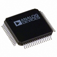
ADV7202KST Analog Devices Inc, ADV7202KST Datasheet - Page 16

ADV7202KST
Manufacturer Part Number
ADV7202KST
Description
IC CODEC VIDEO 10BIT 64LQFP
Manufacturer
Analog Devices Inc
Type
Video Codecr
Datasheet
1.ADV7202KSTZ.pdf
(28 pages)
Specifications of ADV7202KST
Rohs Status
RoHS non-compliant
Data Interface
Serial
Resolution (bits)
12, 10 b
Number Of Adcs / Dacs
1 / 4
Sigma Delta
No
Voltage - Supply, Analog
4.75 V ~ 5.25 V
Voltage - Supply, Digital
4.75 V ~ 5.25 V
Operating Temperature
0°C ~ 70°C
Mounting Type
Surface Mount
Package / Case
64-LQFP
Lead Free Status / Rohs Status
Not Compliant
Available stocks
Company
Part Number
Manufacturer
Quantity
Price
Company:
Part Number:
ADV7202KST
Manufacturer:
CSR
Quantity:
1 000
Company:
Part Number:
ADV7202KSTZ
Manufacturer:
Analog Devices Inc
Quantity:
10 000
ADV7202
MODE REGISTER 0
MR0 (MR07–MR00)
(Address (SR4–SR0) = 00H)
Figure 16 shows the various operations under the control of
Mode Register 0.
MR0 BIT DESCRIPTION
ADC Reference Voltage (MR00)
This control bit is used to select the ADC reference voltage. When
this bit is set to “0,” a reference voltage of 1.1 V is selected. When
the bit is set to “1,” a reference voltage of 2.2 V is selected.
MODE REGISTER 1
MR1 (MR17–MR10)
(Address (SR4–SR0) = 01H)
Figure 17 shows the various operations under the control of
Mode Register 1.
MR1 BIT DESCRIPTION
DAC0 Control (MR10)
Setting this bit to “0” enables DAC0; otherwise, this DAC is
powered down.
DAC1 Control (MR11)
Setting this bit to “0” enables DAC1; otherwise, this DAC is
powered down.
DAC2 Control (MR12)
Setting this bit to “0” enables DAC2; otherwise, this DAC is
powered down.
DAC3 Control (MR13)
Setting this bit to “0” enables DAC3; otherwise, this DAC is
powered down.
MR17
0
1
DAC I/P INVERT
MR07
MR17
DISABLE
ENABLE
MR16
0
1
4:2:2 MODE
ZERO MUST BE
WRITTEN TO
MR07–MR05
THESE BITS
DISABLE
ENABLE
MR06
MR16
MR15
0
1
MR05
MR15
MR04
0
1
MR14
0
1
DUAL CLOCK
DUAL EDGE CLOCK
Figure 16. Mode Register 0
Figure 17. Mode Register 1
POWER-DOWN
SINGLE CLK
DUAL CLK
NORMAL
POWER-DOWN
SINGLE EDGE
DUAL EDGE
MR04
MR14
MR03
0
1
POWER-DOWN
–16–
NORMAL
POWER-DOWN
MR13
MR03
ADC
MR13
0
1
External Reference Enable (MR01)
Setting this bit to “1” enables an external voltage reference for
the ADC.
Voltage Reference Power-Down (MR02)
Setting this bit to “1” causes the internal DAC voltage reference to
power down.
ADC Power-Down (MR03)
Setting this bit to “1” causes the video rate ADC to power down.
Power-Down (MR04)
Setting this bit to “1” puts the device into power-down mode.
Reserved (MR05–MR07)
Zero must be written to these bits.
Dual Edge Clock (MR14)
Setting this bit to “1” allows data to be read into the DACs on
both edges of the clock; hence, data may be read in at twice the
clock frequency. See Figure 17. If this bit is set to “0,” the data
will only be strobed on the rising edge of the clock.
Dual Clock (MR15)
Setting this bit to “1” allows the use of two clocks to strobe data
into the DACs. See Figure 17. It is possible to clock data in
with only one clock and use the second clock to contain timing
information.
4:2:2 Mode (MR16)
Setting this bit to “1” enables data to be input in 4:2:2 format.
4:2:2 mode will only work if MR14 and MR15 register bits are
set to zero.
DAC Input Invert (MR17)
Setting this bit to “1” causes the input data to the DACs to be
inverted allowing for an external inverting amplifier.
DAC3 CONTROL
MR02
0
1
MR12
0
1
NORMAL
POWER-DOWN
POWER-DOWN
DAC2 CONTROL
MR12
MR02
NORMAL
POWER-DOWN
V
NORMAL
POWER-DOWN
REF
MR01
0
1
MR01
MR11
EXT REF
ENABLE
MR11
0
1
INTERNAL
EXTERNAL
DAC1 CONTROL
MR10
0
1
NORMAL
POWER-DOWN
MR10
MR00
DAC0 CONTROL
MR00
0
1
ADC REF
VOLTAGE
NORMAL
POWER-DOWN
1.1V
2.2V
REV. 0


