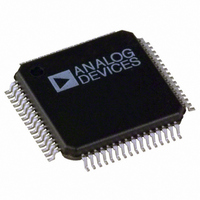
ADV7202KST Analog Devices Inc, ADV7202KST Datasheet - Page 9

ADV7202KST
Manufacturer Part Number
ADV7202KST
Description
IC CODEC VIDEO 10BIT 64LQFP
Manufacturer
Analog Devices Inc
Type
Video Codecr
Datasheet
1.ADV7202KSTZ.pdf
(28 pages)
Specifications of ADV7202KST
Rohs Status
RoHS non-compliant
Data Interface
Serial
Resolution (bits)
12, 10 b
Number Of Adcs / Dacs
1 / 4
Sigma Delta
No
Voltage - Supply, Analog
4.75 V ~ 5.25 V
Voltage - Supply, Digital
4.75 V ~ 5.25 V
Operating Temperature
0°C ~ 70°C
Mounting Type
Surface Mount
Package / Case
64-LQFP
Lead Free Status / Rohs Status
Not Compliant
Available stocks
Company
Part Number
Manufacturer
Quantity
Price
Company:
Part Number:
ADV7202KST
Manufacturer:
CSR
Quantity:
1 000
Company:
Part Number:
ADV7202KSTZ
Manufacturer:
Analog Devices Inc
Quantity:
10 000
Pin No.
1
2
3
4
5
6
7
8–19
20
21
22
23, 24
25
26–35
36
37
38
39
40
41
42
43
44
45
46
47
48
49–52, 55, 56,
59–62
53
54
57, 58
63
64
REV. 0
Mnemonic
SYNC_IN
SCL
ALSB
XTAL0
XTAL1
AVDD_ADC
AVSS_ADC
AIN1–AIN6
DVSS
REFADC
CML
CAP2, CAP1
OSDEN
DOUT[9:0]
OSDIN2
OSDIN1
OSDIN0
DAC3_OUT
DAC2_OUT
AVSS_DAC
AVDD_DAC
DAC1_OUT
DAC0_OUT
COMP
VREFDAC
RSET
RESET
DAC_DATA[9:0]
DVSS
DVDD
DACCLK[1:0]
SYNC_OUT
SDA
Input/
Output
I
I
I
I
O
P
G
I
G
I/O
O
I
I
O
I
I
I
O
O
G
P
O
O
O
I/O
I
I
I
G
P
I
O
I/O
PIN FUNCTION DESCRIPTIONS
Function
This signal can be used to synchronize the updating of clamps. Polarity is pro-
grammable via I
MPU Port Serial Interface Clock Input
This signal sets up the LSB of the MPU address. MPU address = 2cH, ALSB = 0,
MPU address = 2eH, ALSB = 1. When this pin is tied high, the I
which reduces noise on the I
bandwidth on the I
Input terminal for crystal oscillator or connection for external oscillator with
CMOS-compatible square wave clock signal.
Second Terminal for Crystal Oscillator. Not connected if external clock source
is used.
ADC Supply Voltage (5 V or 3.3 V)
Ground for ADC Supply
Analog Signal Inputs. Can be configured differentially or single-ended.
Ground for Digital Core Supply
Voltage Reference Input or Programmable Reference Out.
Common-Mode Level for ADCs. Connect a 0.1 µF capacitor from CML pin to
AVSS_ADC.
ADC Capacitor Network. Connect a 0.1 µF capacitor from each CAP pin to
AVSS_ADC and a 10 µF capacitor across the two CAP pins.
Enable data from OSDIN0–OSDIN2 to be switched to the outputs when set to a logic
high.
ADC Data Output
Third Input Channel for On-Screen Display
Second Input Channel for On-Screen Display
First Input Channel for On-Screen Display
General-Purpose Analog Output
Analog Output. Can be used to output CVBS, R, or U.
Ground for DAC Supply
DAC Supply Voltage (5 V or 3.3 V)
Analog Output. Can be used to output CVBS, Y, G, or Luma.
Analog Output. Can be used to output CVBS, V, B, or Chroma.
Compensation pin for DACs. Connect 0.1 µF capacitor from COMP pin to
AVDD_DAC.
DAC Voltage Reference Output Pin, Nominally 1.235 V. Can be driven by an
external voltage reference.
Used to control the amplitude of the DAC output current, 1200 Ω resistor gives an
I max of 4.33 mA.
Master Reset (Asynchronous)
DAC Input Data for Four Video Rate DACs
Ground for Digital Core Supply
Supply Voltage for Digital Core (5 V or 3.3 V)
DAC Clocks
Output Sync Signal, which goes to a high state while Cr data sample from a
YCrCb data stream or C data from a Y/C data stream is output on DOUT[9:0].
MPU Port Serial Data Input/Output
–9–
2
C.
2
C lines is increased.
2
C interface. When this pin is tied low, the input
2
C filter is activated,
ADV7202


