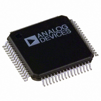
ADV7202KST Analog Devices Inc, ADV7202KST Datasheet - Page 17

ADV7202KST
Manufacturer Part Number
ADV7202KST
Description
IC CODEC VIDEO 10BIT 64LQFP
Manufacturer
Analog Devices Inc
Type
Video Codecr
Datasheet
1.ADV7202KSTZ.pdf
(28 pages)
Specifications of ADV7202KST
Rohs Status
RoHS non-compliant
Data Interface
Serial
Resolution (bits)
12, 10 b
Number Of Adcs / Dacs
1 / 4
Sigma Delta
No
Voltage - Supply, Analog
4.75 V ~ 5.25 V
Voltage - Supply, Digital
4.75 V ~ 5.25 V
Operating Temperature
0°C ~ 70°C
Mounting Type
Surface Mount
Package / Case
64-LQFP
Lead Free Status / Rohs Status
Not Compliant
Available stocks
Company
Part Number
Manufacturer
Quantity
Price
Company:
Part Number:
ADV7202KST
Manufacturer:
CSR
Quantity:
1 000
Company:
Part Number:
ADV7202KSTZ
Manufacturer:
Analog Devices Inc
Quantity:
10 000
MODE REGISTER 2
MR2 (MR20–MR27)
(Address (SR4–SR0) = 02H)
Figure 18 shows the various operations under the control of
Mode Register 2.
MR2 BIT DESCRIPTION
Analog Input Configuration (MR20–MR23)
This control selects the analog input configuration, up to five
CVBS input channels, or two component YUV, or three S-Video
and eight auxiliary inputs. See Figure 18 for details.
SHA0 Control (MR24)
Setting this bit to “0” enables SHA0; otherwise, this SHA is
powered down (SHA = Sample and Hold Amplifier).
MODE REGISTER 3
MR3 (MR30–MR37)
(Address (SR4–SR0) = 03H)
Figure 19 shows the various operations under the control of
Mode Register 3.
MR3 BIT DESCRIPTION
Clamp Current (MR30)
Setting this bit to “1” enables the halving of all clamp currents.
Analog Input Mode (MR31)
Setting this bit to “1” enables differential mode for the analog
inputs; otherwise, the inputs are single-ended. See Figure 19.
SHA Gain (MR32)
Setting this bit to “0” enables SHA gain of 1. If the bit is set to “1,”
the SHA gain is 2. The SHA gain will limit the input signal range.
See Figure 19.
REV. 0
MR27
0
1
AUX CONTROL
MR26
0
1
NORMAL
POWER-DOWN
SHA2 CONTROL
MR27
NORMAL
POWER-DOWN
THESE REGISTERS
MR37
ZERO MUST BE
MR37–MR36
WRITTEN TO
MR26
MR36
MR25
0
1
SHA1 CONTROL
MR25
MR35
0
1
MR35
MR24
0
1
SYNC POLARITY
NORMAL
POWER-DOWN
MR34
0
1
SHA0 CONTROL
OUTPUT ENABLE
LOW
HIGH
Figure 18. Mode Register 2
Figure 19. Mode Register 3
NORMAL
POWER-DOWN
MR24
NORMAL
HIGH Z
MR34
MR23
MR33
–17–
MR33
0
1
VOLTAGE CLAMP
MR23 MR22 MR21 MR20
SHA1 Control (MR25)
Setting this bit to “0” enables SHA1; otherwise, this SHA is
powered down.
SHA2 Control (MR26)
Setting this bit to “0” enables SHA2; otherwise, this SHA is
powered down.
AUX Control (MR27)
Setting this bit to “0” enables the auxiliary ADC; otherwise,
Aux ADC is powered down.
Voltage Clamp (MR33)
Setting this bit to “1” will enable the voltage clamps.
Output Enable (MR34)
Setting this bit to “1” puts the digital outputs into high
impedance.
SYNC Polarity (MR35)
This bit controls the polarity of the SYNC_IN pin. If the bit is set
to “0,” a logic low pulse corresponds to H-Sync. If the bit is “1,”
a logic high pulse corresponds to H-Sync. This sync in pulse can
then be used to control the synchronization of AGC/Clamping.
See AR12.
Reserved (MR36–MR37)
Zero must be written to both these registers.
0
0
0
0
1
1
MR32
0
0
0
0
1
0
1
OFF
ON
MR22
MR32
SHA GAIN
0
0
0
0
1
1
1
1
0
0
0
1
2
ANALOG INPUT CONFIGURATION
0
0
1
1
0
0
1
1
0
0
1
MR21
MR31
0
1
0
1
0
1
0
1
0
1
0
MR31
0
1
ANALOG INPUT
MR30
0
1
SINGLE-ENDED
DIFFERENTIAL
MR20
CVBS IN ON AIN1
CVBS IN ON AIN2
CVBS IN ON AIN3
RESERVED
CVBS IN ON AIN5
CVBS IN ON AIN6
Y/C IN ON AIN1, AIN4
Y/C IN ON AIN2, AIN3
YUV IN ON AIN2, AIN3, AIN6
CVBS IN ON AIN1, 8 AUX INPUTS
CVBS IN ON AIN2, 8 AUX INPUTS
MR30
CLAMP CURRENT
NORMAL
HALF
ADV7202


