SC18IS601IBS,151 NXP Semiconductors, SC18IS601IBS,151 Datasheet - Page 12
SC18IS601IBS,151
Manufacturer Part Number
SC18IS601IBS,151
Description
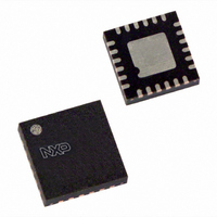
IC SPI TO I2C BUS 24-HVQFN
Manufacturer
NXP Semiconductors
Datasheet
1.SC18IS600IBS151.pdf
(30 pages)
Specifications of SC18IS601IBS,151
Package / Case
24-VQFN Exposed Pad, 24-HVQFN, 24-SQFN, 24-DHVQFN
Controller Type
I²C Bus Controller
Interface
SPI
Voltage - Supply
2.4 V ~ 3.6 V
Current - Supply
11mA
Operating Temperature
-40°C ~ 85°C
Mounting Type
Surface Mount
Maximum Operating Frequency
12 MHz
Maximum Operating Temperature
+ 85 C
Minimum Operating Temperature
- 40 C
Mounting Style
SMD/SMT
Supply Voltage (max)
3.6 V
Supply Voltage (min)
2.4 V
Lead Free Status / RoHS Status
Lead free / RoHS Compliant
For Use With
568-3511 - DEMO BOARD SPI TO I2C
Lead Free Status / Rohs Status
Lead free / RoHS Compliant
Other names
568-4710
935286979151
SC18IS601IBS-S
935286979151
SC18IS601IBS-S


NXP Semiconductors
SC18IS600_601_5
Product data sheet
6.3 External clock input (SC18IS601)
6.4 I
6.5 Serial Peripheral Interface (SPI)
In this device, the processor clock is derived from an external source driving the CLKIN
pin. The clock rate may be from 0 Hz up to 18 MHz.
I
to the bus, and it has the following features:
A typical I
provides a byte-oriented I
(Refer to UM10204, “I
The host communicates with the SC18IS600/601 via the SPI interface. The
SC18IS600/601 operates in Slave mode up to 3 Mbit/s.
The SPI interface has four pins: SCLK, MOSI, MISO, and CS.
Typical connections are shown in
2
2
Fig 11. I
C-bus uses two wires (SDA and SCL) to transfer information between devices connected
•
•
•
•
•
•
•
•
C-bus serial interface
Bidirectional data transfer between masters and slaves
Multi-master bus (no central master)
Arbitration between simultaneously transmitting masters without corruption of serial
data on the bus
Serial clock synchronization allows devices with different bit rates to communicate via
one serial bus
Serial clock synchronization can be used as a handshake mechanism to suspend and
resume serial transfer
The I
SCLK, MOSI and MISO are typically tied together between two or more SPI devices.
Data flows from the master to the SC18IS600/601 on the MOSI (Master Out Slave In)
pin and flows from SC18IS600/601 to the master on the MISO (Master In Slave Out)
pin. The SCLK signal is an input to the SC18IS600/601.
CS is the slave select pin. In a typical configuration, an SPI master selects one SPI
device as the current slave. An SPI slave device uses its CS pin to determine whether
it is selected. The CS pin may be tied LOW if it is the only device on the bus.
2
2
2
C-bus may be used for test and diagnostic purposes.
C-bus configuration is shown in
C-bus configuration
I
2
C-bus
2
C-bus specification and user manual” .)
Rev. 05 — 28 July 2008
SC18IS600/601
2
C-bus interface that supports data transfers up to 400 kHz.
V
DD
Figure
R PU
12.
Figure
I
DEVICE
2
C-BUS
R PU
11. The SC18IS600/601 device
SC18IS600/601
I
DEVICE
2
C-BUS
SPI to I
002aab716
SDA
SCL
© NXP B.V. 2008. All rights reserved.
2
C-bus interface
12 of 30
Related parts for SC18IS601IBS,151
Image
Part Number
Description
Manufacturer
Datasheet
Request
R

Part Number:
Description:
NXP Semiconductors designed the LPC2420/2460 microcontroller around a 16-bit/32-bitARM7TDMI-S CPU core with real-time debug interfaces that include both JTAG andembedded trace
Manufacturer:
NXP Semiconductors
Datasheet:

Part Number:
Description:
NXP Semiconductors designed the LPC2458 microcontroller around a 16-bit/32-bitARM7TDMI-S CPU core with real-time debug interfaces that include both JTAG andembedded trace
Manufacturer:
NXP Semiconductors
Datasheet:
Part Number:
Description:
NXP Semiconductors designed the LPC2468 microcontroller around a 16-bit/32-bitARM7TDMI-S CPU core with real-time debug interfaces that include both JTAG andembedded trace
Manufacturer:
NXP Semiconductors
Datasheet:
Part Number:
Description:
NXP Semiconductors designed the LPC2470 microcontroller, powered by theARM7TDMI-S core, to be a highly integrated microcontroller for a wide range ofapplications that require advanced communications and high quality graphic displays
Manufacturer:
NXP Semiconductors
Datasheet:
Part Number:
Description:
NXP Semiconductors designed the LPC2478 microcontroller, powered by theARM7TDMI-S core, to be a highly integrated microcontroller for a wide range ofapplications that require advanced communications and high quality graphic displays
Manufacturer:
NXP Semiconductors
Datasheet:
Part Number:
Description:
The Philips Semiconductors XA (eXtended Architecture) family of 16-bit single-chip microcontrollers is powerful enough to easily handle the requirements of high performance embedded applications, yet inexpensive enough to compete in the market for hi
Manufacturer:
NXP Semiconductors
Datasheet:
Part Number:
Description:
The XA-S3 device is a member of Philips Semiconductors? XA(eXtended Architecture) family of high performance 16-bitsingle-chip microcontrollers
Manufacturer:
NXP Semiconductors
Datasheet:

Part Number:
Description:
The NXP BlueStreak LH75401/LH75411 family consists of two low-cost 16/32-bit System-on-Chip (SoC) devices
Manufacturer:
NXP Semiconductors
Datasheet:
Part Number:
Description:
The NXP LPC3130/3131 combine an 180 MHz ARM926EJ-S CPU core, high-speed USB2
Manufacturer:
NXP Semiconductors
Datasheet:
Part Number:
Description:
The NXP LPC3141 combine a 270 MHz ARM926EJ-S CPU core, High-speed USB 2
Manufacturer:
NXP Semiconductors
Part Number:
Description:
The NXP LPC3143 combine a 270 MHz ARM926EJ-S CPU core, High-speed USB 2
Manufacturer:
NXP Semiconductors

Part Number:
Description:
The NXP LPC3152 combines an 180 MHz ARM926EJ-S CPU core, High-speed USB 2
Manufacturer:
NXP Semiconductors
Part Number:
Description:
The NXP LPC3154 combines an 180 MHz ARM926EJ-S CPU core, High-speed USB 2
Manufacturer:
NXP Semiconductors

Part Number:
Description:
Standard level N-channel enhancement mode Field-Effect Transistor (FET) in a plastic package using NXP High-Performance Automotive (HPA) TrenchMOS technology
Manufacturer:
NXP Semiconductors
Datasheet: