FIN1047MTC Fairchild Semiconductor, FIN1047MTC Datasheet

IC DRIVER 3.3V LVDS 4BIT 16TSSOP

FIN1047MTC

Manufacturer Part Number
FIN1047MTC
Description
IC DRIVER 3.3V LVDS 4BIT 16TSSOP
Manufacturer
Fairchild Semiconductor
Type
Driverr
Datasheet

Specifications of FIN1047MTC

Number Of Drivers/receivers
4/0
Protocol
LVDS
Voltage - Supply
3 V ~ 3.6 V
Mounting Type
Surface Mount
Package / Case
16-TSSOP
Logic Family
FIN10
Logic Type
High Speed Differential Driver
Supply Voltage (max)
3.6 V
Supply Voltage (min)
3 V
Maximum Operating Temperature
+ 85 C
Mounting Style
SMD/SMT
Data Rate
400 Mbps
Interface
EIA/TIA-644
Minimum Operating Temperature
- 40 C
Number Of Lines (input / Output)
1 / 1
Supply Current
22 mA
Lead Free Status / RoHS Status
Lead free / RoHS Compliant

Available stocks

Company
Part Number
Manufacturer
Quantity
Price
Part Number:
FIN1047MTCX
Manufacturer:
FAIRCHILD/仙童
Quantity:
20 000
Company:
Part Number:
FIN1047MTCX
Quantity:
64
© 2003 Fairchild Semiconductor Corporation
FIN1047M
FIN1047MTC
FIN1047
3.3V LVDS 4-Bit Flow-Through
High Speed Differential Driver
General Description
This quad driver is designed for high speed interconnects
utilizing Low Voltage Differential Signaling (LVDS) technol-
ogy. The driver translates LVTTL signal levels to LVDS lev-
els with a typical differential output swing of 350mV which
provides low EMI at ultra low power dissipation even at
high frequencies. This device is ideal for high speed trans-
fer of clock and data.
The FIN1047 can be paired with its companion receiver,
the FIN1048, or any other LVDS receiver.
Ordering Code:
Devices also available in Tape and Reel. Specify by appending the suffix letter “X” to the ordering code.
Connection Diagram
Truth Table
H
X
Order Number
L or OPEN
HIGH Logic Level L
Don’t Care
EN
H
H
H
X
L or OPEN
L or OPEN
L or OPEN
Inputs
EN
H
X
Package Number
Z
LOW Logic Level
High Impedance
MTC16
M16A
OPEN
D
H
X
X
L
IN
16-Lead Small Outline Integrated Circuit (SOIC), JEDEC MS-012, 0.150" Narrow
16-Lead Thin Shrink Small Outline Package (TSSOP), JEDEC MO-153, 4.4mm Wide
D
OUT
H
L
L
Z
Z
Outputs
DS500589
D
OUT
H
H
Z
Z
L
Features
Pin Descriptions
Greater than 400Mbs data rate
Flow-through pinout simplifies PCB layout
3.3V power supply operation
0.4 ns maximum differential pulse skew
1.7 ns maximum propagation delay
Low power dissipation
Power-Off protection
Meets or exceeds the TIA/EIA-644 LVDS standard
Pin compatible with equivalent RS-422 and LVPECL
devices
16-Lead SOIC and TSSOP packages save space
D
D
OUT1
OUT1
Package Description
D
, D
, D
IN1
OUT2
OUT2
, D
Pin Name
IN2
GND
V
EN
EN
, D
, D
, D
CC
IN3
OUT3
OUT3
, D
IN4
, D
, D
OUT4
OUT4
June 2001
Revised August 2003
LVTTL Data Inputs
Non-Inverting
Driver Outputs
Inverting
Driver Outputs
Driver Enable Pin
Inverting Driver
Enable Pin
Power Supply
Ground
www.fairchildsemi.com
Description

Related parts for FIN1047MTC

FIN1047MTC Summary of contents

Page 1

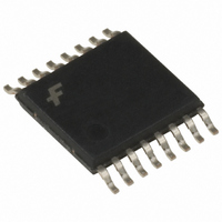
... FIN1047M M16A 16-Lead Small Outline Integrated Circuit (SOIC), JEDEC MS-012, 0.150" Narrow FIN1047MTC MTC16 16-Lead Thin Shrink Small Outline Package (TSSOP), JEDEC MO-153, 4.4mm Wide Devices also available in Tape and Reel. Specify by appending the suffix letter “X” to the ordering code. ...

Page 2

Absolute Maximum Ratings Supply Voltage ( Input Voltage ( Input Voltage (V ) OUT Driver Short Circuit Current (I ) OSD Storage Temperature Range (T ) STG Max Junction Temperature ( Lead ...

Page 3

AC Electrical Characteristics Over supply voltage and operating temperature ranges, unless otherwise specified Symbol Parameter t Differential Propagation Delay PLHD LOW-to-HIGH t Differential Propagation Delay PHLD HIGH-to-LOW t Differential Output Rise Time (20% to 80%) TLHD t Differential Output Fall ...

Page 4

FIGURE 1. Differential Driver DC Test Circuit FIGURE 3. AC Waveforms FIGURE 5. Enable and Disable AC Waveforms www.fairchildsemi.com Note A: All input pulses have frequency 10 MHz Note B: C includes all fixture and instrumentation capacitance L ...

Page 5

Typical Performance Curves FIGURE 7. Output High Voltage vs. Power Supply Voltage FIGURE 9. Output Short Circuit Current vs. Power Supply Voltage FIGURE 11. Differential Output Voltage vs. Load Resistor FIGURE 8. Output Low Voltage vs. Power ...

Page 6

Typical Performance Curves FIGURE 13. Power Supply Current vs. Frequency FIGURE 15. Power Supply Current vs. Ambient Temperature FIGURE 17. Differential Propagation Delay vs. Ambient Temperature www.fairchildsemi.com (Continued) FIGURE 14. Power Supply Current vs. Power Supply Voltage ...

Page 7

Typical Performance Curves FIGURE 19. Differential Pulse Skew (t PLH Ambient Temperature (Continued vs. FIGURE 20. Transition Time vs. PHL Power Supply Voltage FIGURE 21. Transition Time vs. Ambient Temperature 7 www.fairchildsemi.com ...

Page 8

Physical Dimensions inches (millimeters) unless otherwise noted 16-Lead Small Outline Integrated Circuit (SOIC), JEDEC MS-012, 0.150" Narrow www.fairchildsemi.com Package Number M16A 8 ...

Page 9

Physical Dimensions Physical Dimensions inches (millimeters) unless otherwise noted (Continued) inches (millimeters) unless otherwise noted (Continued) 16-Lead Thin Shrink Small Outline Package (TSSOP), JEDEC MO-153, 4.4mm Wide Fairchild does not assume any responsibility for use of any circuitry described, no ...

Related keywords