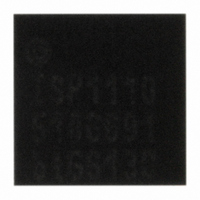
ISP1110VHTS ST-Ericsson Inc, ISP1110VHTS Datasheet - Page 20

ISP1110VHTS
Manufacturer Part Number
ISP1110VHTS
Description
IC USB TXRX W/UART 16-HBCC
Manufacturer
ST-Ericsson Inc
Type
Transceiverr
Datasheet
1.ISP1110VHTS.pdf
(26 pages)
Specifications of ISP1110VHTS
Number Of Drivers/receivers
1/1
Protocol
USB 2.0
Voltage - Supply
4 V ~ 5.5 V
Mounting Type
Surface Mount
Package / Case
16-HBCC
Lead Free Status / RoHS Status
Lead free / RoHS Compliant
Other names
568-3149-2
ISP1110VH-G
ISP1110VH-G
Available stocks
Company
Part Number
Manufacturer
Quantity
Price
Company:
Part Number:
ISP1110VHTS
Manufacturer:
AD
Quantity:
1 954
Part Number:
ISP1110VHTS
Manufacturer:
ST-ERICS
Quantity:
20 000
NXP Semiconductors
ISP1110_2
Product data sheet
15.1 Introduction to soldering
15.2 Wave and reflow soldering
15.3 Wave soldering
15.4 Reflow soldering
Soldering is one of the most common methods through which packages are attached to
Printed Circuit Boards (PCBs), to form electrical circuits. The soldered joint provides both
the mechanical and the electrical connection. There is no single soldering method that is
ideal for all IC packages. Wave soldering is often preferred when through-hole and
Surface Mount Devices (SMDs) are mixed on one printed wiring board; however, it is not
suitable for fine pitch SMDs. Reflow soldering is ideal for the small pitches and high
densities that come with increased miniaturization.
Wave soldering is a joining technology in which the joints are made by solder coming from
a standing wave of liquid solder. The wave soldering process is suitable for the following:
Not all SMDs can be wave soldered. Packages with solder balls, and some leadless
packages which have solder lands underneath the body, cannot be wave soldered. Also,
leaded SMDs with leads having a pitch smaller than ~0.6 mm cannot be wave soldered,
due to an increased probability of bridging.
The reflow soldering process involves applying solder paste to a board, followed by
component placement and exposure to a temperature profile. Leaded packages,
packages with solder balls, and leadless packages are all reflow solderable.
Key characteristics in both wave and reflow soldering are:
Key characteristics in wave soldering are:
Key characteristics in reflow soldering are:
•
•
•
•
•
•
•
•
•
•
•
Through-hole components
Leaded or leadless SMDs, which are glued to the surface of the printed circuit board
Board specifications, including the board finish, solder masks and vias
Package footprints, including solder thieves and orientation
The moisture sensitivity level of the packages
Package placement
Inspection and repair
Lead-free soldering versus PbSn soldering
Process issues, such as application of adhesive and flux, clinching of leads, board
transport, the solder wave parameters, and the time during which components are
exposed to the wave
Solder bath specifications, including temperature and impurities
Lead-free versus SnPb soldering; note that a lead-free reflow process usually leads to
higher minimum peak temperatures (see
reducing the process window
Rev. 02 — 19 March 2007
Figure
USB transceiver with UART signaling
14) than a PbSn process, thus
© NXP B.V. 2007. All rights reserved.
ISP1110
19 of 25


