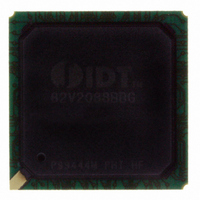
IDT82V2088BBG IDT, Integrated Device Technology Inc, IDT82V2088BBG Datasheet - Page 17

IDT82V2088BBG
Manufacturer Part Number
IDT82V2088BBG
Description
IC LINE INTERFACE UNIT 208-PBGA
Manufacturer
IDT, Integrated Device Technology Inc
Type
Line Interface Units (LIUs)r
Datasheet
1.IDT82V2088BBG.pdf
(78 pages)
Specifications of IDT82V2088BBG
Protocol
E1
Voltage - Supply
3.13 V ~ 3.47 V
Mounting Type
Surface Mount
Package / Case
208-PBGA
Screening Level
Industrial
Mounting
Surface Mount
Operating Temperature (min)
-40C
Operating Temperature (max)
85C
Lead Free Status / RoHS Status
Lead free / RoHS Compliant
Number Of Drivers/receivers
-
Lead Free Status / RoHS Status
Compliant, Lead free / RoHS Compliant
Other names
800-1705
82V2088BBG
82V2088BBG
Available stocks
Company
Part Number
Manufacturer
Quantity
Price
Company:
Part Number:
IDT82V2088BBG
Manufacturer:
IDT
Quantity:
22
Company:
Part Number:
IDT82V2088BBG
Manufacturer:
IDT
Quantity:
784
Company:
Part Number:
IDT82V2088BBG
Manufacturer:
IDT, Integrated Device Technology Inc
Quantity:
10 000
Part Number:
IDT82V2088BBG
Manufacturer:
IDT
Quantity:
20 000
OCTAL CHANNEL T1/E1/J1 LONG HAUL/SHORT HAUL LINE INTERFACE UNIT
‘0111’.
3.2.3.2 LBO (Line Build Out)
be attenuated before transmission for long haul applications. The FCC Part
68 Regulations specifies four grades of attenuation with a step of 7.5 dB.
Three LBOs are used to implement the pulse attenuation. The PULS[3:0]
bits (TCF1, 03H...) are used to select the attenuation grade. Both
and
3.2.3.3 User-Programmable Arbitrary Waveform
waveform generator mode can be used in the corresponding channel. This
allows the transmitter performance to be tuned for a wide variety of line con-
dition or special application.
UI[1:0] bits (TCF3, 05H...) and each UI is divided into 16 sub-phases,
addressed by the SAMP[3:0] bits (TCF3, 05H...). The pulse amplitude of
each phase is represented by a binary byte, within the range from +63 to -
63, stored in WDAT[6:0] bits (TCF4, 06H...) in signed magnitude form. The
most positive number +63 (D) represents the maximum positive amplitude
of the transmit pulse while the most negative number -63 (D) represents the
maximum negative amplitude of the transmit pulse. Therefore, up to 64
bytes are used. For each channel, a 64 bytes RAM is available.
User can select one of them as reference and make some changes to get
the desired waveform.
pulse shape. In order to do this, firstly, users can choose a set of waveform
value from the following twelve tables, which is the most similar to the
desired pulse shape. Table-2, Table-3, Table-4, Table-5, Table-6, Table-7,
Table-8, Table-9, Table-10, Table-11,
data and scaling data of each of the twelve templates. Then modify the cor-
responding sample data to get the desired transmit pulse shape.
Note: R
For J1 applications, the PULS[3:0] (TCF1, 03H...) should be set to
To prevent the cross-talk at the far end, the output of TTIP/TRING could
When the PULS[3:0] bits are set to ‘11xx’, user-programmable arbitrary
Each pulse shape can extend up to 4 UIs (Unit Interval), addressed by
There are twelve standard templates which are stored in a local ROM.
User can change the wave shape and the amplitude to get the desired
IDT82V2088
Table-15
Table-14
LOAD
Figure-7 T1 Pulse Template Test Circuit
= 100 Ω ± 5%
list these values.
lists these values.
TRINGn
TTIPn
Table-12
Cable
and
Table-13
list the sample
R
LOAD
Table-14
V
OUT
17
by 1, the pulse amplitude can be scaled up or down at the percentage ratio
against the standard pulse amplitude if needed. For different pulse shapes,
the value of SCAL[5:0] bits and the scaling percentage ratio are different.
The following twelve tables list these values.
grammed, based on the selected waveform template:
from the internal RAM.
lap of two consecutive pulses could make the pulse amplitude overflow
(exceed the maximum limitation) if the pulse amplitude is not set properly.
This overflow is captured by DAC_OV_IS bit (INTS1, 17H...), and, if
enabled by the DAC_OV_IM bit (INTM1, 12H...), an interrupt will be gen-
erated.
templates and LBOs in detail for reference. For preset pulse templates and
LBOs, scaling up/down against the pulse amplitude is not supported.
Secondly, through the value of SCAL[5:0] bits increased or decreased
Do the followings step by step, the desired waveform can be pro-
(1).Select the UI by UI[1:0] bits (TCF3, 05H...)
(2).Specify the sample address in the selected UI by SAMP [3:0] bits
(3).Write sample data to WDAT[6:0] bits (TCF4, 06H...). It contains the
(4).Set the RW bit (TCF3, 05H...) to ‘0’ to implement writing data to RAM,
(5).Implement the Read from RAM/Write to RAM by setting the DONE
Repeat the above steps until all the sample data are written to or read
(6).Write the scaling data to SCAL[5:0] bits (TCF2, 04H...) to scale the
When more than one UI is used to compose the pulse template, the over-
The following tables give all the sample data based on the preset pulse
1.Table-2
2.Table-3
3.Table-4
4.Table-5
5.Table-6
6.Table-7
7.Table-8
8.Table-9
9.Table-10
10.Table-11
11.Table-12
12.Table-13
(TCF3, 05H...)
data to be stored in the RAM, addressed by the selected UI and the
corresponding sample address.
or to ‘1’ to implement read data from RAM
bit (TCF3, 05H...)
amplitude of the waveform based on the selected standard pulse
amplitude
Transmit Waveform Value For E1 75 Ω
Transmit Waveform Value For E1 120 Ω
Transmit Waveform Value For T1 0~133 ft
Transmit Waveform Value For T1 133~266 ft
Transmit Waveform Value For T1 266~399 ft
Transmit Waveform Value For T1 399~533 ft
Transmit Waveform Value For T1 533~655 ft
Transmit Waveform Value For J1 0~655 ft
Transmit Waveform Value For DS1 0 dB LBO
Transmit Waveform Value For DS1 -7.5 dB LBO
Transmit Waveform Value For DS1 -15.0 dB LBO
Transmit Waveform Value For DS1 -22.5 dB LBO
TEMPERATURE RANGES
INDUSTRIAL


