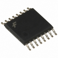
FIN1047MTCX Fairchild Semiconductor, FIN1047MTCX Datasheet - Page 3

FIN1047MTCX
Manufacturer Part Number
FIN1047MTCX
Description
IC DRIVER 3.3V LVDS 4BIT 16TSSOP
Manufacturer
Fairchild Semiconductor
Type
Driverr
Datasheet
1.FIN1047MTC.pdf
(9 pages)
Specifications of FIN1047MTCX
Number Of Drivers/receivers
4/0
Protocol
LVDS
Voltage - Supply
3 V ~ 3.6 V
Mounting Type
Surface Mount
Package / Case
16-TSSOP
Logic Family
FIN10
Logic Type
High Speed Differential Driver
Supply Voltage (max)
3.6 V
Supply Voltage (min)
3 V
Maximum Operating Temperature
+ 85 C
Mounting Style
SMD/SMT
Data Rate
400 Mbps
Interface
EIA/TIA-644
Minimum Operating Temperature
- 40 C
Number Of Lines (input / Output)
1 / 1
Supply Current
22 mA
Lead Free Status / RoHS Status
Lead free / RoHS Compliant
Available stocks
Company
Part Number
Manufacturer
Quantity
Price
Part Number:
FIN1047MTCX
Manufacturer:
FAIRCHILD/仙童
Quantity:
20 000
t
t
t
t
t
t
t
t
f
t
t
t
t
C
C
PLHD
PHLD
TLHD
THLD
SK(P)
SK(LH)
SK(HL)
SK(PP)
MAX
ZHD
ZLD
HZD
LZD
AC Electrical Characteristics
Over supply voltage and operating temperature ranges, unless otherwise specified
Note 4: All typical values are at T
Note 5: t
tion.
Note 6: t
(either LOW-to-HIGH or HIGH-to-LOW) when both devices operate with the same supply voltage, same temperature, and have identical test circuits.
Note 7: f
Note 8: Test Circuits in Figures 2, 4, 6 are simplified representations of test fixture and DUT loading.
IN
OUT
Symbol
SK(LH)
SK(PP)
MAX
Differential Propagation Delay
LOW-to-HIGH
Differential Propagation Delay
HIGH-to-LOW
Differential Output Rise Time (20% to 80%)
Differential Output Fall Time (80% to 20%)
Pulse Skew |t
Channel-to-Channel Skew
(Note 5)
Part-to-Part Skew (Note 6)
Maximum Frequency (Note 7)
Differential Output Enable Time from Z to HIGH
Differential Output Enable Time from Z to LOW R
Differential Output Disable Time from HIGH to Z See Figure 4 (Note 8), and Figure 5
Differential Output Disable Time from LOW to Z
Input Capacitance
Output Capacitance
criteria: Input t
, t
is the magnitude of the difference in propagation delay times between any specified terminals of two devices switching in the same direction
SK(HL)
is the skew between specified outputs of a single device when the outputs have identical loads and are switching in the same direc-
R
PLH
t
F
- t
Parameter
A
PHL
1ns, 0V to 3V, 50% Duty Cycle; Output V
25 C and with V
|
CC
3.3V.
R
See Figure 2 (Note 8), and Figure 3
R
L
L
L
100 , C
100 , See Figure 6 (Note 8)
100 , C
OD
Test Conditions
3
L
250 mv, 45% to 55% Duty Cycle; all switching in phase channels.
L
10 pF,
10 pF,
Min
200
0.6
0.6
0.4
0.4
(Note 4)
0.05
Typ
250
1.1
1.2
1.7
1.7
2.7
2.7
4.2
5.2
www.fairchildsemi.com
Max
1.7
1.7
1.2
1.2
0.4
0.3
1.0
5.0
5.0
5.0
5.0
Units
MHz
ns
ns
ns
ns
ns
ns
ns
ns
ns
ns
ns
pF
pF


