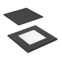
CYP15G0401DXB-BGXC Cypress Semiconductor Corp, CYP15G0401DXB-BGXC Datasheet - Page 11

CYP15G0401DXB-BGXC
Manufacturer Part Number
CYP15G0401DXB-BGXC
Description
IC TXRX HOTLINK 256LBGA
Manufacturer
Cypress Semiconductor Corp
Series
HOTlink II™r
Type
Transceiverr
Specifications of CYP15G0401DXB-BGXC
Package / Case
256-LBGA Exposed Pad, 32-HLBGA
Number Of Drivers/receivers
4/4
Protocol
Multiprotocol
Voltage - Supply
3.135 V ~ 3.465 V
Mounting Type
Surface Mount
Product
PHY
Data Rate
1500 MBd
Supply Voltage (max)
3.465 V
Supply Voltage (min)
3.135 V
Supply Current
1.06 A
Maximum Operating Temperature
+ 70 C
Minimum Operating Temperature
0 C
Mounting Style
SMD/SMT
Number Of Channels
4
Lead Free Status / RoHS Status
Lead free / RoHS Compliant
For Use With
CYP15G0401DX-EVAL - IC TXRX HOTLINK 256-BGA
Lead Free Status / Rohs Status
Lead free / RoHS Compliant
Available stocks
Company
Part Number
Manufacturer
Quantity
Price
Company:
Part Number:
CYP15G0401DXB-BGXC
Manufacturer:
Cypress Semiconductor Corp
Quantity:
135
Company:
Part Number:
CYP15G0401DXB-BGXC
Manufacturer:
Cypress
Quantity:
465
Company:
Part Number:
CYP15G0401DXB-BGXC
Manufacturer:
CYPRESS
Quantity:
748
Company:
Part Number:
CYP15G0401DXB-BGXC
Manufacturer:
Cypress Semiconductor Corp
Quantity:
10 000
Document #: 38-02002 Rev. *L
Pin Descriptions
CYP(V)(W)15G0401DXB Quad HOTLink II Transceiver
RXCLKA±
RXCLKB±
RXCLKC±
RXCLKD±
RXCKSEL
Pin Name
Three-state, LVTTL
Output clock or static
control input
Three-level Select
static control input
I/O Characteristics
(continued)
[5]
,
Receive Character Clock Output or Clock Select Input. When configured such that
all output data paths are clocked by the recovered clock (RXCKSEL = MID), these
true and complement clocks are the receive interface clocks which are used to control
timing of output data (RXDx[7:0], RXSTx[2:0] and RXOPx). These clocks are output
continuously at either the dual-character rate (1/20
rate (1/10
When configured such that all output data paths are clocked by REFCLK instead of a
recovered clock (RXCKSEL = LOW), the RXCLKA± and RXCLKC± output drivers
present a buffered and delayed form of REFCLK. RXCLKA± and RXCLKC± are
buffered forms of REFCLK that are slightly different in phase. This phase difference
allows the user to select the optimal setup/hold timing for their specific interface.
When RXCKSEL = LOW and quad channel bonding is enabled, RXCLKB+ and
RXCLKD+ are static control inputs used to select the master channel for bonding and
status control.
When RXCKSEL = HIGH and quad-channel bonding is enabled, one of the recovered
clocks from channels A, B, C or D can be selected to clock the bonded output data.
The selection of the recovered clock is made by RXCLKB+ and RXCLKD+ which act
as static control inputs in this mode. Both RXCLKA± and RXCLKC± output buffered
forms of the recovered clock selected from receive channel A, B, C, or D. See Table 15
for details.
When RXCKSEL = HIGH and dual-channel bonding is enabled, one of the recovered
clocks from channels A or B is selected to present bonded data from channels A and
B, and one of the recovered clocks from channels C or D is selected to present bonded
data from channels C and D. RXCLKA± output the recovered clock from either receive
channel A or receive channel B as selected by RXCLKB+ to clock the bonded output
data from channels A and B, and RXCLKC± output the recovered clock from either
receive channel C or receive channel D as selected by RXCLKD+ to the clock the
bonded output data from channels C and D. See Table 16 for details.
Receive Clock Mode. Selects the receive clock source used to transfer data to the
Output Registers.
When LOW, all four Output Registers are clocked by REFCLK. RXCLKB± and
RXCLKD± outputs are disabled (High-Z), and RXCLKA± and RXCLKC± present
buffered and delayed forms of REFCLK. This clocking mode is required for channel
bonding across multiple devices.
When MID, each RXCLKx± output follows the recovered clock for the respective
channel, as selected by RXRATE. When the 10B/8B Decoder and Elasticity Buffer are
bypassed (DECMODE = LOW), RXCKSEL must be MID.
When HIGH and channel bonding is enabled in dual-channel mode (RX modes 3 and
5), RXCLKA± outputs the recovered clock from either receive channel A or B as
selected by RXCLKB+, and RXCLKC± outputs the recovered clock from either receive
channel C or D as selected by RXCLKD+. These output clocks may operate at the
character-rate or half the character-rate as selected by RXRATE.
When HIGH and channel bonding is enabled in quad channel mode (RX modes 6 and
8), or if the receive channels are operated in independent mode (RX modes 0 and 2),
RXCLKA± and RXCLKC± output the recovered clock from receive channel A, B, C,
or D, as selected by RXCLKB+ and RXCLKD+. This output clock may operate at the
character-rate or half the character-rate as selected by RXRATE.
th
the serial bit-rate) of the data being received, as selected by RXRATE.
Signal Description
th
the serial bit-rate) or character
CYW15G0401DXB
CYP15G0401DXB
CYV15G0401DXB
Page 11 of 53


