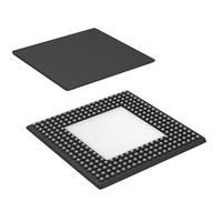
CYP15G0401DXB-BGXC Cypress Semiconductor Corp, CYP15G0401DXB-BGXC Datasheet - Page 52

CYP15G0401DXB-BGXC
Manufacturer Part Number
CYP15G0401DXB-BGXC
Description
IC TXRX HOTLINK 256LBGA
Manufacturer
Cypress Semiconductor Corp
Series
HOTlink II™r
Type
Transceiverr
Specifications of CYP15G0401DXB-BGXC
Package / Case
256-LBGA Exposed Pad, 32-HLBGA
Number Of Drivers/receivers
4/4
Protocol
Multiprotocol
Voltage - Supply
3.135 V ~ 3.465 V
Mounting Type
Surface Mount
Product
PHY
Data Rate
1500 MBd
Supply Voltage (max)
3.465 V
Supply Voltage (min)
3.135 V
Supply Current
1.06 A
Maximum Operating Temperature
+ 70 C
Minimum Operating Temperature
0 C
Mounting Style
SMD/SMT
Number Of Channels
4
Lead Free Status / RoHS Status
Lead free / RoHS Compliant
For Use With
CYP15G0401DX-EVAL - IC TXRX HOTLINK 256-BGA
Lead Free Status / Rohs Status
Lead free / RoHS Compliant
Available stocks
Company
Part Number
Manufacturer
Quantity
Price
Company:
Part Number:
CYP15G0401DXB-BGXC
Manufacturer:
Cypress Semiconductor Corp
Quantity:
135
Company:
Part Number:
CYP15G0401DXB-BGXC
Manufacturer:
Cypress
Quantity:
465
Company:
Part Number:
CYP15G0401DXB-BGXC
Manufacturer:
CYPRESS
Quantity:
748
Company:
Part Number:
CYP15G0401DXB-BGXC
Manufacturer:
Cypress Semiconductor Corp
Quantity:
10 000
Document #: 38-02002 Rev. *L
Document History Page
REV.
Document Title: CYP(V)(W)15G0401DXB Quad HOTLink II™ Transceiver
Document Number: 38-02002
*G
*A
*B
*C
*D
*E
*F
**
105840 03/21/01
108025 06/20/01
108437 07/19/01
112986 11/12/01
118650 09/30/02
121906 02/12/03
124996 03/21/03
ECN
No.
2/26/02
Issue
Date
Change
Orig. of
AMV
TME
LNM
CGX
TPS
TPS
POT
SZV
Change from Spec number: 38-00876 to 38-02002
Changed Marketing part number
Change Marketing part number from CYP15G0401DX to CYP15G0401
Changed common mode input information and duty cycle of transmit clocks
Updated max voltage power and release under ecn control
Changed the wording of REFCLK input coupling on both inputs for LVTTL clock input
Addition of TXCLKO+ and the TXCLKO+ specs
Changed the TXCLKO clock output to refect the new timing
Changed the Half Clock drawing so that the viald time was at clock edges
Changed the input power
Changed the spec for the serial output levels at the different terminations
Changed the common mode input range of the serial input
Increased the Serial input current under the conditions of VCC and min
Added to the Duty cycle of the transmit and receiver clock signals
The rise time of the serial inputs and receiver were changed
The half rate timing drawing changed from not valid at clock edges to viald at clock edges
Added new timing line for status valid time of half clock signals
Max voltage reduced from 4.2V to 3.8V
Matched the common specs with the family of parts
Changed many names from lower case to upper case
Changed in five places = to ≠
Changed the power to typical to 2.8W
Added Escon, DVB-ASI, SMPTE to features
Under PARCTL control reworded statement When HIGH
Under RXLE Reworded and reformatted the text
Under BOND_ALL added when bonding resolution is completed
Removed repeated information in Power Control section
Corrected statement for bonded BIST
Changed TXCLKO description
Changed TXPERx description
Changed typical power from 2.8W to 2.9W
Removed the LOW setting for FRAMCHAR and related references
Changed V
Changed the I
Changed the t
Changed t
Changed t
Changed the JTAG ID from 0C800069 to 1C800069
Changed Minimum tRISE/tFALL for CML
Changed tRXLOCK
Changed tDJ, tRJ
Changed tJTOL
Changed tTXLOCK
Changed tRXCLKH, tRXCLKL
Changed tTXCLKOD+, tTXCLKOD
Changed Power Specs
Changed verbiage...Paragraph: Clock/Data Recovery
Changed verbiage...Paragraph: Range Control
Added Power-up Requirements
Changed CYP15G0401DXB to CYP(V)15G0401DXB to abbreviate title. Type corre-
sponding to the Video compliant parts
Reduced the lower limit of the serial signaling rate from 200 Mbaud to 195 Mbaud and
changed the associated specifications accordingly
Added CYPV15G0401DXB to title
TXDS
REFADV–
ODIF
OST
TXCLKR
& t
and V
TXDH
boundary values
and t
OLC
and t
and t
REFCDV–
for CML output
TXCLKF
TREFDS
Description of Change
min. values
& t
TREFDH
CYW15G0401DXB
CYP15G0401DXB
CYV15G0401DXB
Page 52 of 53


