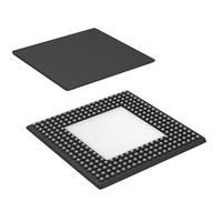
CYP15G0401DXB-BGXC Cypress Semiconductor Corp, CYP15G0401DXB-BGXC Datasheet - Page 27

CYP15G0401DXB-BGXC
Manufacturer Part Number
CYP15G0401DXB-BGXC
Description
IC TXRX HOTLINK 256LBGA
Manufacturer
Cypress Semiconductor Corp
Series
HOTlink II™r
Type
Transceiverr
Specifications of CYP15G0401DXB-BGXC
Package / Case
256-LBGA Exposed Pad, 32-HLBGA
Number Of Drivers/receivers
4/4
Protocol
Multiprotocol
Voltage - Supply
3.135 V ~ 3.465 V
Mounting Type
Surface Mount
Product
PHY
Data Rate
1500 MBd
Supply Voltage (max)
3.465 V
Supply Voltage (min)
3.135 V
Supply Current
1.06 A
Maximum Operating Temperature
+ 70 C
Minimum Operating Temperature
0 C
Mounting Style
SMD/SMT
Number Of Channels
4
Lead Free Status / RoHS Status
Lead free / RoHS Compliant
For Use With
CYP15G0401DX-EVAL - IC TXRX HOTLINK 256-BGA
Lead Free Status / Rohs Status
Lead free / RoHS Compliant
Available stocks
Company
Part Number
Manufacturer
Quantity
Price
Company:
Part Number:
CYP15G0401DXB-BGXC
Manufacturer:
Cypress Semiconductor Corp
Quantity:
135
Company:
Part Number:
CYP15G0401DXB-BGXC
Manufacturer:
Cypress
Quantity:
465
Company:
Part Number:
CYP15G0401DXB-BGXC
Manufacturer:
CYPRESS
Quantity:
748
Company:
Part Number:
CYP15G0401DXB-BGXC
Manufacturer:
Cypress Semiconductor Corp
Quantity:
10 000
Document #: 38-02002 Rev. *L
In this mode, the BOND_ALL signal of all bonding devices
must be connected together. The BOND_ALL signal is a wired
AND and the signal is LOW during the bonding resolution
process. After the completion of bonding resolution it returns
HIGH.
Power Control
The CYP(V)(W)15G0401DXB supports user control of the
powered up or down state of each transmit and receive
channel. The receive channels are controlled by the RXLE
signal and the values present on the BOE[7:0] bus. The
transmit channels are controlled by the OELE signal and the
values present on the BOE[7:0] bus. Powering down unused
channels will save power and reduce system heat generation.
Controlling system power dissipation will improve the system
performance.
Receive Channels
When RXLE is HIGH, the signals on the BOE[7:0] inputs
directly control the power enables for the receive PLLs and
analog circuits. When a BOE[7:0] input is HIGH, the
associated receive channel [A through D] PLL and analog
logic are active. When a BOE[7:0] input is LOW, the
associated receive channel [A through D] PLL and analog
circuits are powered down. When RXLE returns LOW, the last
values present on the BOE[7:0] inputs are captured in the
Receive Channel Enable Latch. The specific BOE[7:0] input
signal associated with a receive channel is listed in Table 10.
If a single channel of a bonded-pair or quad is disabled, this
may prevent the other receive channels from bonding. If the
disabled channel has been selected as the master channel for
insert/delete functions, or for recovered clock select, these
functions will not operate. Any disabled receive channel will
indicate a constant LFIx output.
When a disabled receive channel is re-enabled, the status of
the associated LFIx output and data on the parallel outputs for
the associated channel may be indeterminate for up to 2 ms.
Transmit Channels
When OELE is HIGH, the signals on the BOE[7:0] inputs
directly control the power enables for the Serial Drivers. When
a BOE[x] input is HIGH, the associated Serial Driver is
enabled. When a BOE[x] input is LOW, the associated Serial
Driver is disabled and powered down. If both Serial Drivers of
a channel are disabled, the internal logic for that transmit
channel is powered down. When OELE returns LOW, the
values present on the BOE[7:0] inputs are latched in the
Output Enable Latch.
Device Reset State
When the CYP(V)(W)15G0401DXB is reset by assertion of
TRSTZ, the Transmit Enable and Receive Enable Latches are
both cleared, and the BIST Enable Latch is preset. In this
state, all transmit and receive channels are disabled, and BIST
is disabled on all channels.
Following a device reset, it is necessary to enable the transmit
and receive channels used for normal operation. This can be
done by sequencing the appropriate values on the BOE[7:0]
Notes:
18. The RXOPx outputs are also driven from the associated Output Register, but their interpretation is under the separate control of PARCTL.
inputs while the OELE and RXLE signals are raised and
lowered. For systems that do not require dynamic control of
power, or want the device to power up in a fixed configuration,
it is also possible to strap the RXLE and OELE control signals
HIGH to permanently enable their associated latches.
Connection of the associated BOE[7:0] signals to a stable
HIGH will then enable the respective transmit and receive
channels as soon as the TRSTZ signal is deasserted.
Output Bus
Each receive channel presents a 12-signal output bus
consisting of
The bit assignments of the Data and Status are dependent on
the setting of DECMODE. The bits are assigned as per
Table 17.
Table 17. Output Register Bit Assignments
When the 10B/8B Decoder is bypassed (DECMODE = LOW),
the framed 10-bit character and a single status bit (COMDET)
are presented at the receiver Output Register. The status
output indicates if the character in the Output Register is one
of the selected framing characters. The bit usage and mapping
of the external signals to the raw 10B transmission character
is shown in Table 18.
The COMDETx outputs are HIGH when the character in the
Output Register for the associated channel contains the
selected framing character at the proper character boundary,
and LOW for all other bit combinations.
When the Low-Latency Framer and half-rate receive port
clocking are also enabled (RFMODE = LOW, RXRATE =
HIGH, and RXCKSEL ≠ LOW), the Framer will stretch the
recovered clock to the nearest 20-bit boundary such that the
rising edge of RXCLKx+ occurs when COMDETx is present on
the associated output bus.
• an eight-bit data bus
• a three-bit status bus
• a parity bit.
RXSTx[2]
RXDx[7]
Signal Name
RXSTx[1]
RXSTx[0]
RXDx[0]
RXDx[1]
RXDx[2]
RXDx[3]
RXDx[4]
RXDx[5]
RXDx[6]
(MSB)
(LSB)
DECMODE = LOW
COMDETx
DOUTx[0]
DOUTx[1]
DOUTx[9]
DOUTx[2]
DOUTx[3]
DOUTx[4]
DOUTx[5]
DOUTx[6]
DOUTx[7]
DOUTx[8]
CYW15G0401DXB
CYP15G0401DXB
CYV15G0401DXB
DECMODE = MID or
RXSTx[2]
RXSTx[1]
RXSTx[0]
RXDx[0]
RXDx[1]
RXDx[2]
RXDx[3]
RXDx[4]
RXDx[5]
RXDx[6]
RXDx[7]
Page 27 of 53
[18]
HIGH


