TDGL003 Microchip Technology, TDGL003 Datasheet - Page 207
TDGL003
Manufacturer Part Number
TDGL003
Description
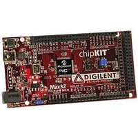
ChipKIT Max32 Development Board PIC32 Boards And Kits
Manufacturer
Microchip Technology
Series
PIC® 32MXr
Type
MCUr
Specifications of TDGL003
Silicon Manufacturer
Microchip
Core Architecture
MIPS
Core Sub-architecture
PIC32
Silicon Core Number
PIC32MX
Silicon Family Name
PIC32MX795Fxxxx
Kit Contents
Board Only
Contents
Board
Lead Free Status / Rohs Status
Lead free / RoHS Compliant
For Use With/related Products
MPLAB®, Arduino™ Mega


Revision H (May 2011)
The revision includes the following global update:
• All references to V
• Added references to the new V-Temp temperature
This revision also includes minor typographical and
formatting changes throughout the data sheet text.
Major updates are referenced by their respective
section in the following table.
TABLE A-3:
© 2011 Microchip Technology Inc.
Section 1.0 “Device Overview”
Section 4.0 “Memory Organization”
Section 5.0 “Flash Program Memory”
Section 8.0 “Oscillator Configuration”
Section 11.0 “USB On-The-Go (OTG)”
Section 16.0 “Output Compare”
Section 22.0 “10-bit Analog-to-Digital
Converter (ADC)”
Section 26.0 “Special Features”
changed to: V
range: -40ºC to +105ºC
Section Name
CORE
MAJOR SECTION UPDATES
DDCORE
/V
CAP
/V
CAP
have been
Updated the V
Added Note 2 and changed the RIPL<2:0> bits to SRIPL<2:0> in the
Interrupt Register Map tables (see
Added Note 2 to the Timer1-5 Register Map (see
Updated the All Resets value for I2C1CON<15:0> and I2C2CON<15:0>
in the I2C1 and I2C2 Register Map (see
Updated the All Resets value for SPI1STAT<15:0> and SPI2STAT<15:0>
in the SPI1 and SPI2 Register Map (see
Updated the All Resets value for CM1CON<15:0> and CM2CON<15:0>
in the Comparator Register Map (see
Renamed the RCDIV<2:0> bits to FRCDIV<2:0> and the LOCK bit to
SLOCK in the OSCCON register, and added Note 3 and the
SYSKEYregister to the System Control Registers Map (see
Updated the All Resets value for the PMSTAT register in the Parallel
Master Port Register Map (see
Updated the All Resets value for CHECON<15:0> and CHETAG<15:0>
in the Prefetch Register Map (see
Renamed FUPLLEN, FUPLLIDIV, and FPLLMULT in the DEVCFG2
register to: UPLLEN, UPLLIDIV, and FPLLMUL, respectively in the
Device Configuration Word Summary (see
Added Notes 1 through 4 to the USB Register Map (see
Added a note on Flash LVD Delay and
Updated the PIC32MX3XX/4XX Family Clock Diagram (see
Updated the PIC32MX3XX/4XX Family USB Interface Diagram (see
Figure
Updated the Output Compare Module Block Diagram (see
Updated the ADC Conversion Clock Period Block Diagram (see
Figure
Renamed FUPLLEN, FUPLLIDIV, and FPLLMULT in the DEVCFG2
register to: UPLLEN, UPLLIDIV, and FPLLMUL, respectively (see
Register
11-1).
22-2).
26-3).
BUS
description in
Update Description
PIC32MX3XX/4XX
Table
Table 1-1: “Pinout I/O
Table
Table 4-2
4-37).
Table
Example
4-39).
Table
Table
Table
4-17).
through
4-10).
4-12).
5-1.
4-41).
Table
Table
DS61143H-page 207
4-7).
Descriptions”.
Table
Figure
4-6.
Table
Figure
4-43).
16-1).
4-20).
8-1).
Related parts for TDGL003
Image
Part Number
Description
Manufacturer
Datasheet
Request
R

Part Number:
Description:
Manufacturer:
Microchip Technology Inc.
Datasheet:
Part Number:
Description:
Manufacturer:
Microchip Technology Inc.
Datasheet:
Part Number:
Description:
Manufacturer:
Microchip Technology Inc.
Datasheet:
Part Number:
Description:
Manufacturer:
Microchip Technology Inc.
Datasheet:
Part Number:
Description:
Manufacturer:
Microchip Technology Inc.
Datasheet:
Part Number:
Description:
Manufacturer:
Microchip Technology Inc.
Datasheet:
Part Number:
Description:
Manufacturer:
Microchip Technology Inc.
Datasheet:
Part Number:
Description:
Manufacturer:
Microchip Technology Inc.
Datasheet: