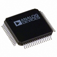
ADV7343BSTZ Analog Devices Inc, ADV7343BSTZ Datasheet - Page 66

ADV7343BSTZ
Manufacturer Part Number
ADV7343BSTZ
Description
IC ENCODER VIDEO W/DAC 64-LQFP
Manufacturer
Analog Devices Inc
Type
Video Encoderr
Datasheet
1.ADV7343BSTZ.pdf
(104 pages)
Specifications of ADV7343BSTZ
Applications
DVD, Blu-Ray
Voltage - Supply, Analog
3.3V
Voltage - Supply, Digital
1.8V
Mounting Type
Surface Mount
Package / Case
64-LQFP
Supply Voltage Range
1.71V To 1.89V
Operating Temperature Range
-40°C To +85°C
Tv / Video Case Style
LQFP
No. Of Pins
64
Svhc
No SVHC (18-Jun-2010)
Operating Temperature Max
85°C
Operating
RoHS Compliant
Input Format
Digital
Output Format
Analogue
Dac Resolution
11bit
Rohs Compliant
Yes
Lead Free Status / RoHS Status
Lead free / RoHS Compliant
Available stocks
Company
Part Number
Manufacturer
Quantity
Price
Company:
Part Number:
ADV7343BSTZ
Manufacturer:
ADI
Quantity:
301
Company:
Part Number:
ADV7343BSTZ
Manufacturer:
Analog Devices Inc
Quantity:
10 000
Part Number:
ADV7343BSTZ
Manufacturer:
ADI/亚德诺
Quantity:
20 000
Company:
Part Number:
ADV7343BSTZ-3
Manufacturer:
ADI
Quantity:
246
ADV7342/ADV7343
EXTERNAL HORIZONTAL AND VERTICAL SYNCHRONIZATION CONTROL
For timing synchronization purposes, the ADV7342/ADV7343 are able to accept either EAV/SAV time codes embedded in the input
pixel data or external synchronization signals provided on the S_HSYNC , S_VSYNC , P_HSYNC , P_VSYNC , and P_BLANK pins (see
Table 55
Table 55. Timing Synchronization Signal Input Options
Signal
SD HSYNC In
SD VSYNC/FIELD In
ED/HD HSYNC In
ED/HD VSYNC/FIELD In
ED/HD BLANK In
1
Table 56. Timing Synchronization Signal Output Options
Signal
SD HSYNC Out
SD VSYNC/FIELD Out
ED/HD HSYNC Out
ED/HD VSYNC/FIELD Out
1
Table 57. S_HSYNC Output Control
ED/HD Input Sync
Format
(Subaddress
0x30, Bit 2)
X
X
0
1
X
1
2
SD and ED/HD timing synchronization outputs must also be disabled (Subaddress 0x02[7:6] = 00).
ED/HD timing synchronization outputs must also be disabled (Subaddress 0x02, Bit 7 = 0).
In all ED/HD standards where there is an HSYNC output, the start of the HSYNC pulse is aligned with the falling edge of the embedded HSYNC in the output video.
X = don’t care.
). It is also possible to output synchronization signals on the
ED/HD HSYNC
Control
(Subaddress
0x34, Bit 1)
X
X
0
0
1
Pin
S_HSYNC
S_VSYNC
P_HSYNC
P_VSYNC
P_BLANK
Pin
S_HSYNC
S_VSYNC
S_HSYNC
S_VSYNC
1, 2
ED/HD Sync
Output Enable
(Subaddress
0x02, Bit 7)
0
0
1
1
1
Condition
SD slave timing mode (1, 2, or 3) selected (Subaddress 0x8A[2:0])
SD slave timing mode (1, 2, or 3) selected (Subaddress 0x8A[2:0])
ED/HD timing synchronization inputs enabled (Subaddress 0x30, Bit 2 = 0)
ED/HD timing synchronization inputs enabled (Subaddress 0x30, Bit 2 = 0)
Condition
SD timing synchronization outputs enabled (Subaddress 0x02, Bit 6 = 1)
SD timing synchronization outputs enabled (Subaddress 0x02, Bit 6 = 1)
ED/HD timing synchronization outputs enabled (Subaddress 0x02, Bit 7 = 1)
ED/HD timing synchronization outputs enabled (Subaddress 0x02, Bit 7 = 1)
SD Sync
Output Enable
(Subaddress
0x02, Bit 6)
0
1
X
X
X
Rev. A | Page 66 of 104
S_HSYNC and S_VSYNC pins (see
Signal on S_HSYNC Pin
Tristate
Pipelined SD HSYNC
Pipelined ED/HD HSYNC
Pipelined ED/HD HSYNC based on
AV Code H bit
Pipelined ED/HD HSYNC based on
horizontal counter
Table 56
1
1
Duration
N/A
See the
As per HSYNC timing.
Same as line blanking
interval.
Same as embedded
HSYNC.
to
1
1
Table 58
SD Timing
).
section.


