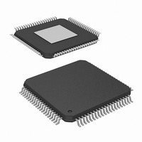
HMP8117CNZ Intersil, HMP8117CNZ Datasheet - Page 24

HMP8117CNZ
Manufacturer Part Number
HMP8117CNZ
Description
IC VIDEO DECODER NTSC/PAL 80PQFP
Manufacturer
Intersil
Type
Video Decoderr
Datasheet
1.HMP8117CNZ.pdf
(45 pages)
Specifications of HMP8117CNZ
Applications
Video
Voltage - Supply, Analog
4.75 V ~ 5.25 V
Voltage - Supply, Digital
4.75 V ~ 5.25 V
Mounting Type
Surface Mount
Package / Case
80-MQFP, 80-PQFP
Lead Free Status / RoHS Status
Lead free / RoHS Compliant
Available stocks
Company
Part Number
Manufacturer
Quantity
Price
NUMBER
NO.
BIT
BIT
1-0
7
6
5
4
3
2
1
0
7
6
5
4
3
2
Video Data
Output Enable
Video Timing
Output Enable
FIELD Polarity
BLANK Polarity
HSYNC Polarity
VSYNC Polarity
DVALID Polarity
VBIVALID Polarity
Aspect Ratio
Mode
Freeze Output
Timing Enable
DVALID Duty Cycle
Control
(DVLD_DCYC)
DVALID Line Timing
Control
(DVLD_LTC)
Missing HSYNC
Detect Select
Missing VSYNC
Detect Select
CLK2 Frequency
FUNCTION
FUNCTION
24
This bit is used to enable the P0-P15 outputs.
0 = Outputs 3-stated. 1 = Outputs enabled
This bit is used to enable the HSYNC, VSYNC, BLANK, FIELD, VBIVALID, DVALID, and
INTREQ outputs. 0 = Outputs 3-stated. 1 = Outputs enabled
0 = Active low (low during odd fields). 1 = Active high (high during odd fields)
0 = Active low (low during blanking). 1 = Active high (high during blanking)
0 = Active low (low during horizontal sync). 1 = Active high (high during horizontal sync)
0 = Active low (low during vertical sync). 1 = Active high (high during vertical sync)
0 = Active low (low during valid pixel data). 1 = Active high (high during valid pixel data)
0 = Active low (low during VBI data). 1 = Active high (high during VBI data)
0 = Rectangular (BT.601) pixels
1 = Square pixels
Setting this bit to a “1” freezes the output timing at the end of the field. Resetting this bit to a “0”
resumes normal operation at the start of the next field.
0 = Normal operation
1 = Freeze output timing
This bit is ignored during the 8-bit YCbCr and BT.656 output modes.
During 16-bit YCbCr, 15-bit RGB, or 16-bit RGB output modes, this bit is defined as:
0 = DVALID has 50/50 duty cycle at the pixel output data rate
1 = DVALID goes active based on line-lock. This will cause DVALID to not have a 50/50 duty
cycle. This bit is intended to be used in maintaining backward compatibility with the HMP8112A
DVALID output timing.
During 16-bit YCbCr, 15-bit RGB, or 16-bit RGB output modes, this bit is defined as:
0 = DVALID present only during active video time on active scan lines
1 = DVALID present the entire scan line time on all scan lines
During the 8-bit YCbCr and BT.656 output modes, this bit defines the DVALID output as:
0 = Normal timing
1 = DVALID signal ANDed with CLK2
This bit specifies the number of missing horizontal sync pulses before entering horizontal lock
acquisition mode.
0 = 12 pulses
1 = 1 pulse
This bit specifies the number of missing vertical sync pulses before entering vertical lock
acquisition mode.
0 = 3 pulses
1 = 1 pulse
This bit indicates the frequency of the CLK2 input clock.
00 = 24.54MHz10 = 29.5MHz
01 = 27.0MHz11 = Reserved
TABLE 15. GENLOCK CONTROL REGISTER
TABLE 14. OUTPUT CONTROL REGISTER
SUB ADDRESS = 03
SUB ADDRESS = 04
HMP8117
DESCRIPTION
DESCRIPTION
H
H
April 19, 2007
RESET
RESET
STATE
STATE
01
0
0
0
0
0
0
0
0
0
0
0
0
1
0
FN4643.3
B
B
B
B
B
B
B
B
B
B
B
B
B
B
B


