HMP8117CNZ Intersil, HMP8117CNZ Datasheet - Page 9
HMP8117CNZ
Manufacturer Part Number
HMP8117CNZ
Description
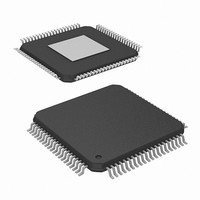
IC VIDEO DECODER NTSC/PAL 80PQFP
Manufacturer
Intersil
Type
Video Decoderr
Datasheet
1.HMP8117CNZ.pdf
(45 pages)
Specifications of HMP8117CNZ
Applications
Video
Voltage - Supply, Analog
4.75 V ~ 5.25 V
Voltage - Supply, Digital
4.75 V ~ 5.25 V
Mounting Type
Surface Mount
Package / Case
80-MQFP, 80-PQFP
Lead Free Status / RoHS Status
Lead free / RoHS Compliant
Available stocks
Company
Part Number
Manufacturer
Quantity
Price


Built-in Video Generation
The decoder can be configured to output a full-screen of built-in
blue, black or 75% color bar patterns. The type of pattern
generated is determined by bits 2-1 of the OUTPUT FORMAT
register 02
bits need to be set for normal operation to pass decoded video.
If the decoder is currently locked to a video source on the
input, the output data timing will be based on the input video
source. If an input video source is not detected, internally-
generated output data timing will be used. The following
table lists the data codes output for each built-in video
pattern in YCbCr format.
for gamma = 2.2:
for gamma = 2.8:
NTSC(M) LINE#
PAL(M) LINE#
PATTERN: COLOR
for R′B′ < 0.0812*31, G′ < 0.0812*63
for R′B′ >= 0.0812*31, G′ >= 0.0812*63
R = (31)(R′/31)
G = (63)(G′/63)
B = (31)(B′/31)
TABLE 2. BUILT-IN VIDEO PATTERN DATA CODES
HSYNC
VSYNC
VIDEO
INPUT
FIELD
75% Color Bar: White
R = (31)((R′/31)/4.5)
G = (63)((G′/63)/4.5)
B = (31)((B′/31)/4.5)
R = (31)(((R′/31) + 0.099)/1.099)
G = (63)(((G′/63) + 0.099)/1.099)
B = (31)(((B′/31) + 0.099)/1.099)
Black Screen: Black
H
. When built-in video generation is not desired, the
Blue Screen: Blue
524
521
Magenta
2.8
2.8
2.8
Yellow
Green
Black
Cyan
Blue
Red
525
522
9
B4
A2
4B
83
70
54
41
23
10
10
Y
H
H
H
H
H
H
H
H
H
H
523
‘EVEN’ FIELD
1
FIGURE 3. NTSC(M) AND PAL(M) ODD FIELD TIMING
2.2
2.2
2.2
2C
9C
D4
D9
80
48
B8
64
80
80
Cb
H
H
H
H
H
H
H
H
H
H
524
2
8E
2C
3A
C6
D4
80
72
80
88
80
Cr
525
H
H
H
H
H
H
H
H
H
H
3
HMP8117
1
4
Pixel Port Timing
The the timing and format of the output data and control
signals is presented in the following sections. Refer to the
section “CYCLE SLIPPING AND REAL-TIME PIXEL
JITTER” for PLL and interface considerations.
HSYNC and VSYNC Timing
The HSYNC and VSYNC output timing is VMI v1.4 compatible.
Figures 3-6 illustrate the video timing. The leading edge of
HSYNC is synchronous to the video input signal and has a
fixed latency due to internal pipeline processing. The pulse
width of the HSYNC is defined by the END HSYNC register
36
delay of 0-510 CLK2 cycles from the leading edge.
The leading edge of VSYNC is asserted approximately half way
through the first serration pulse of each field. An accumulator is
used to detect a low-time period within the serration pulse.
Since the leading edge of VSYNC is detected, it should not be
used for timing with respect to HSYNC or BLANK.
The trailing edge of VSYNC implements the VMI handshake
with HSYNC in order to determine field information without
using the FIELD pin. For an odd field, the trailing edge of
VSYNC is 5
HSYNC that follows the last equalization pulse. Refer to
Figures 3 and 5. For an even field, the trailing edge of VSYNC
is 5
follows the last equalization pulse. Refer to Figures 4 and 6.
Field Timing
When field information can be determined from the input
video source, the FIELD output pin reflects the video source
field state. When field information cannot be determined
from the input video source, the FIELD output pin alternates
its state at the beginning of each field. FIELD changes state
5
±
H
1 CLK2 cycles before the leading edge of VSYNC.
‘ODD’ FIELD
, where the trailing edge of HSYNC has a programmable
±
1 CLK2 cycles after the leading edge of the HSYNC that
2
5
±
1 CLK2 cycles after the trailing edge of the
6
3
4
7
5
8
9
6
10
7
April 19, 2007
FN4643.3
Related parts for HMP8117CNZ
Image
Part Number
Description
Manufacturer
Datasheet
Request
R

Part Number:
Description:
Ntsc/pal Video Decoder
Manufacturer:
Intersil Corporation
Datasheet:
Part Number:
Description:
Intersil Corporation [CMOS Serial Controller Interface]
Manufacturer:
Intersil Corporation
Datasheet:
Part Number:
Description:
Manufacturer:
Intersil Corporation
Datasheet:
Part Number:
Description:
357-036-542-201 CARDEDGE 36POS DL .156 BLK LOPRO
Manufacturer:
Intersil Corporation
Datasheet:
Part Number:
Description:
1024-Word x 4-Bit LSI Static RAM
Manufacturer:
Intersil Corporation
Datasheet:
Part Number:
Description:
General Purpose NPN Transistor Arrays FN341.4
Manufacturer:
Intersil Corporation
Datasheet:
Part Number:
Description:
CMOS 16-Bit Microprocessor
Manufacturer:
Intersil Corporation
Datasheet:
Part Number:
Description:
Manufacturer:
Intersil Corporation
Datasheet:
Part Number:
Description:
Manufacturer:
Intersil Corporation
Datasheet:
Part Number:
Description:
Manufacturer:
Intersil Corporation
Datasheet:
Part Number:
Description:
Manufacturer:
Intersil Corporation
Datasheet:
Part Number:
Description:
CMOS 6-Bit Latch and Decoder Memory Interfaces
Manufacturer:
Intersil Corporation
Datasheet:
Part Number:
Description:
CA3046General Purpose NPN Transistor Arrays
Manufacturer:
Intersil Corporation
Datasheet:
Part Number:
Description:
Manufacturer:
Intersil Corporation
Datasheet:
Part Number:
Description:
TR909 DLC/FLC SLIC with Low Power Standby
Manufacturer:
Intersil Corporation
Datasheet: